Enrique C Samano
Scientific Tracks Abstracts: J Material Sci Eng
Artificial DNA nanostructures such as DNA origami have garnered significant interest as templates for sub-20 nm assembly of materials because their design allows for the incorporation of binding sites to assemble nanocomponents with 6 nm resolution. In addition, their overall size of 100 nm is easily accessible by top-down lithographic methods. A commercially viable route for fabricating electronic and photonic devices with nanometer-scale features may be pursued by combining the strengths of top-down lithography and bottom-up self-assembly using DNA nanostructures. Electron beam lithography (EBL) is a prime top-down technique used to write a pattern on a substrate, usually a dielectric material. Among many other applications, it is employed to localize and isolate specific nanostructures for future experiments. This is done by two different ways: 1) Creating a pattern composed of several features in order to use them as an alignment mark to localize a unique nanostructure in the microscope. 2) Creating an array of apertures, or ?windows?, with a size slightly larger than the nanostructures to be positioned. A series of patterns on SiOx substrates to place DNA origami nanostructures, before and after metallization, with a rectangular shape (70 � 90 nm) are presented. The main goal of this work is the isolation and alignment of metallic nanostructures.
Enrique C Samano earned his PhD degree in Physics from Stevens Institute of Technology in Hoboken, NJ. He is currently a Research Professor at Centro de Nanociencias y Nanotecnolog�a at UNAM in Ensenada, BC, Mexico, working on thin film growth and surface science techniques. He has been a Visiting Scholar at University of Southern California and recently at Duke University in the DNA Nanotechnology Group. He works on the fabrication of nanostructures based on DNA with applications in electronics and plasmonics. He has published more than 30 papers in reputed journals and is serving as symposiums organizer.
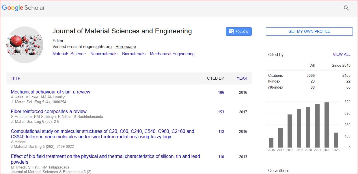
Journal of Material Sciences & Engineering received 3677 citations as per Google Scholar report


 Spanish
  Chinese
  Russian
  German
  French
  Japanese
  Portuguese
  Hindi
Hindi 