Toshihide Nabatame
Scientific Tracks Abstracts: Material Sci Eng
Atomic layer deposition (ALD) technique has been widely investigated to achieve the requirements of atomic-level controllability and conformal growth on three-dimensional structure for a wide range of semiconductor application. Indeed, future scaling of Complementary Metal-Oxide-Semiconductor and charge trap flash memory require new materials as gate insulator and charge tarp layer, respectively. Ionic oxides such as Al2O3, TiO2, and (Ta/Nb)Ox have promising candidates because of a high dielectric constant (high-k) value and large band gap. We present characteristic of each layer and Al2O3/(Ta/ Nb)Ox/Al2O3 multi-layer fabricated by a low temperature process using ALD. The anatase TiO2 and (Ta/Nb)Ox thin films are negligible small charge and have significant high k value of about 30. We found that charge trap capacitors with Al2O3/(Ta/Nb) Ox/Al2O3 multi-layer show superior electrical properties and trapping mechanism of high-k layer as a charge trap layer.
Toshihide Nabatame received his PhD in Engineering in 1994 from Tokyo Institute of Technology and worked at Hitachi Ltd and Renesas Technology Co. He is manager of MANA Foundry in NIMS, Japan. His research interest is to find and fabricate functional devices with metal oxide thin film for future semiconductor region.
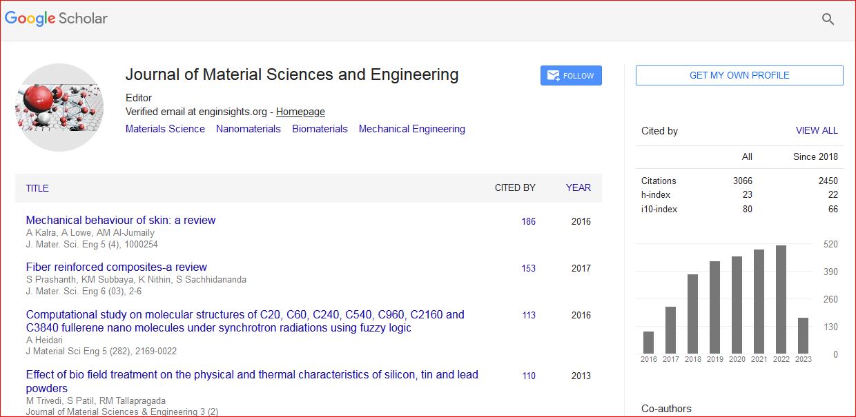
Journal of Material Sciences & Engineering received 3677 citations as per Google Scholar report


 Spanish
  Chinese
  Russian
  German
  French
  Japanese
  Portuguese
  Hindi
Hindi 