Tetsuo Kodera
Scientific Tracks Abstracts: J Material Sci Eng
For the purpose of development of novel functional devices such as quantum information devices, single electron transistors, and sensitive sensors, quantum dots (QDs) attract a great deal of attention. We develop experimentally and theoretically various QD device structures in Si [1-4]. In order to fabricate lithographically-defined Si QDs, we utilize electron beam lithography, reactive ion etching, and oxidation, in a metal-oxide-semiconductor (MOS) structure on a non-doped silicon-oninsulator (SOI) substrate. We apply the fabrication process of Si MOS technologies into our QD devices. We study both n-channel and p-channel Si QD devices. We clearly observed Coulomb oscillation, which is the evidence of single carrier tunneling. Charge detection of change in number of carriers (electrons for n-channel QDs and holes for p-channel QDs) in QDs, one by one, has been successfully demonstrated using the device where we attached single QDs as charge sensors in the vicinity of the double QDs. Few-electron and few-hole regimes in QDs are also realized in n- channel and p- channel QD devices, respectively. These achievements are the important steps for realizing quantum information devices, single electron transistors, and sensitive sensors. This work was financially supported by Grants-in-Aid (Kakenhi Nos. 24102703, 26709023, and 26630151), the PRESTO program of the Japan Science and Technology Agency (JST), the Yazaki Memorial Foundation for Science and Technology, and the Project for Developing Innovation Systems of the Ministry of Education, Culture, Sports, Science and Technology (MEXT) of Japan.
Tetsuo Kodera has completed his doctorate in physics at the age of 27 years at the University of Tokyo. He worked as a Research Associate at the University of Tokyo, and an Assistant Professor at Tokyo Institute of Technology. He is an Associate Professor at Department of Physical Electronics, Tokyo Institute of Technology. He has published more than 40 papers in reputed journals. He was the recipient of the Presentation Award of the Japan Society of Applied Physics, and The Young Scientists? Prize of The Commendation for Science and Technology by the Minister of Education, Culture, Sports, Science and Technology.
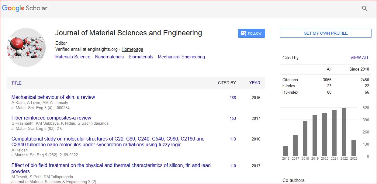
Journal of Material Sciences & Engineering received 3677 citations as per Google Scholar report


 Spanish
  Chinese
  Russian
  German
  French
  Japanese
  Portuguese
  Hindi
Hindi 