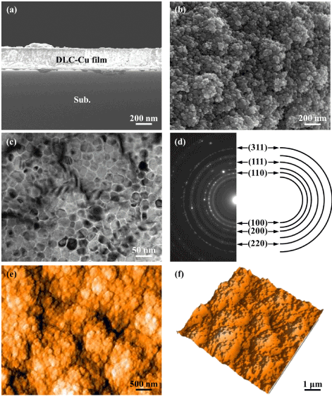
Figure 1:
SEM (a) cross-section and (b) top view images of the DLC-Cu thin film (c) TEM and (d) the selected area electron diffraction pattern; AFM (e) 2D and (f) 3D images of the DLC-Cu thin film.