Felix Gunkel
Aachen University, Germany
Scientific Tracks Abstracts: J Material Sci Eng
Perovskite oxides exhibit a plethora of fascinating electronic material properties covering an exceptionally wide range of phenomena in solid state and surface physics. This has led to tremendous efforts to functionalize these materials in applications for energy technology, gas sensing, and electronics. Layered in an atomically defined epitaxial heterostructures and superlattices, diverse properties of perovskites can be combined on the nanoscale level. In such structures, even new functionality can arise at interfaces of layered materials, exhibiting properties that are absent in the bare bulk materials. In our approach, we utilize atomically-defined layer growth to obtain desired material properties. However, on top of that, we employ thermodynamic engineering of crystal defects as a unique approach to functionalize material properties at surfaces and interfaces: Even at material synthesis conditions close to perfection, device properties are often determined by imperfection, hence, by lattice disorder and crystal defects. As we discuss, we can intentionally control defect structure in nanoscale devices, by developing and utilizing thermodynamic routes to trigger surface and interface reactions in confined systems. While historically defects were seen as something to be avoided, a change of paradigm is required in the field of complex oxides today: In these materials, we can promote functionality, such as metallicity in nominally insulating compounds, by atomic defect-management. Therefore, rather than avoiding defect formation, it is an essential necessity to control and to utilize defect formation in oxides on the nanoscale. Here, we discuss fundamental aspects of lattice disorder effects in bulk oxides, and elaborate the special character of defect formation in thin films, surfaces and interfaces. Focusing on SrTiO3 as a perovskite model system, we will crosslink fundamental perspectives on lattice disorder to actual applications, addressing different examples, such as resistive switching memories, high-mobility electron gases and induced magnetism, oxygen sensors, and electro-catalysts. Recent Publications:�? 1. F. Gunkel, et al., â�?�?Defect-control of anomalous and conventional electron transport in NdGaO3/SrTiO3 heterostructuresâ�?, Physical Review X, 6, 031035 (2016) 2. F. Gunkel et al., â�?�?Ordering and phase control in epitaxial (Pr,Ba)CoO3-ï¤ catalysts for oxygen evolution reactionâ�?, ACS Catalysis 7 (10), 7029â�?�?7037 (2017) 3. M. Andr�?¤ et al., â�?�?Oxygen partial pressure dependence of space charge formation in donor doped SrTiO3â�?, APL Materials 5, 056106 (2017) 4. F. Gunkel et al., â�?�?Mobility modulation and suppression of defect-formation in two-dimensional electron systems by charge transfer managementâ�?, ACS Applied Materials & interfaces 9 (12), 10888 (2017) 5. R. Meyer et al., â�?�?Dynamics of the metal-insulator transition of donor-doped SrTiO3â�?, Physical Review B 94, 115408 (2016) 6. F. Gunkel et al., â�?�?Defect concentration profiles at complex oxide interfacesâ�?, Physical Review B 93, 245431 (2016).
Felix Gunkel is a young investigator based at Institute of Electronic Materials (IWE2) at RWTH Aachen University, Germany. His research interests comprise thermodynamics and solid state chemistry of complex oxides on the nanoscale. His current work addresses tailored functionality of crystal defects in oxides for nano-electronic devices, energy applications, and gas sensors. With background is fundamental and applied physics, Dr. Gunkel started his scientific career at Institute of Solid State Physics, Forschungszentrum Jülich, Jülich, Germany in 2010. He received his PhD from the faculty of electronic engineering at RWTH Aachen University in 2013. After continuing his scientific work in his postdoctoral career at Stanford University and Forschungszentrum Jülich, he is now leading a research team at RWTH Aachen University, Germany, with a research focus of thermodynamic engineering of device properties and material functionality on the nanoscale.
Email:gunkel@iwe.rwth-aachen.de
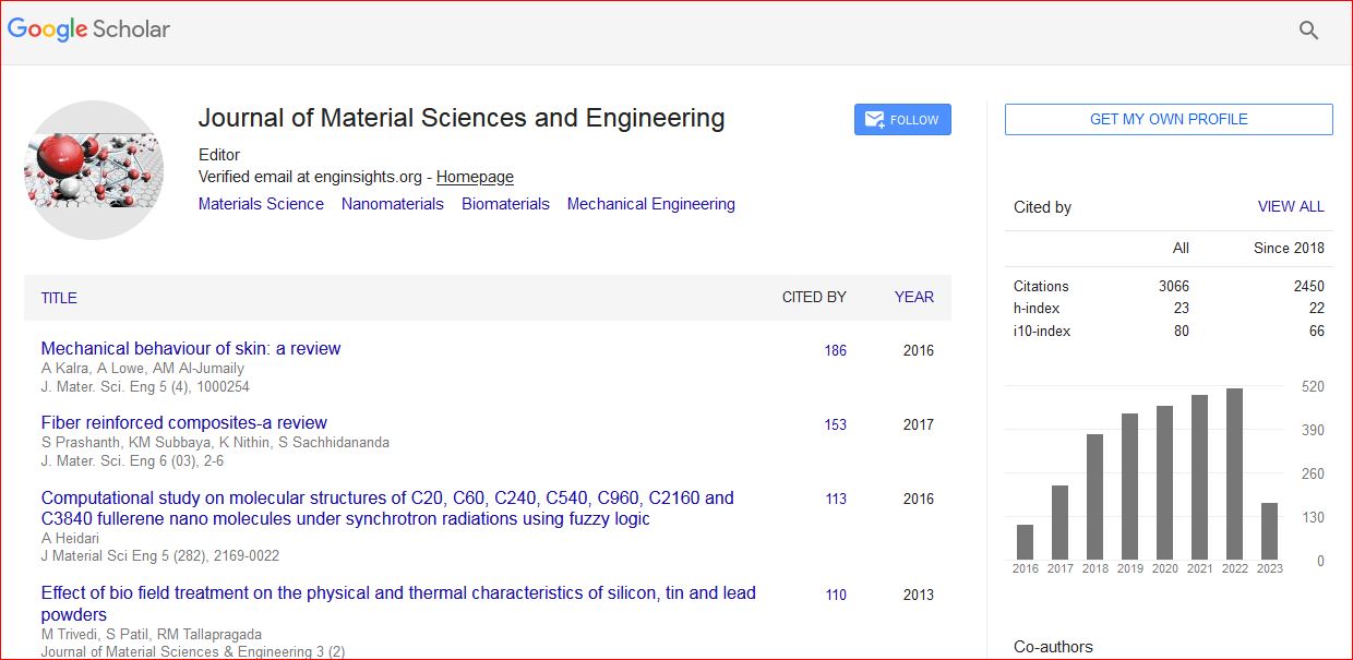
Journal of Material Sciences & Engineering received 3677 citations as per Google Scholar report


 Spanish
  Chinese
  Russian
  German
  French
  Japanese
  Portuguese
  Hindi
Hindi 