Y. Al-Douri, Abdulwahab S. Z. Lahewil, N. M. Ahmed and U. Hashim
Accepted Abstracts: J Material Sci
High quality CdS nanostructures deposited on n-type Silicon wafers at 200, 400, 500 and 600 o C by sol-gel spin coating method without a catalyst are prepared. CdS nanostructures have been characterized by scanning electron microscopy (SEM) and atomic force microscopy (AFM) to research the topography and morphology of the nanostructures. Also, they have been analyzed using X-ray diffraction (XRD); the grin size, full width half maxima, miller indices, strain, dislocation density, lattice constant, interplaner distance and number of crystelinity are measured and bulk modulus is calculated using our model and Fourier transform infrared (FTIR). Photoluminescence (PL) spectroscopy is used to measure the energetic transitions for calculating the refractive index and optical dielectric constant by specific models. Ultra violet (UV-vis) spectroscopy is utilized to study absorption, reflection and extinction coefficient. Thermogravimetric analysis (TGA), differential thermal analysis (DTA) and differential scanning calorimetry (DSC) are to analyze the electrical and thermal properties of antireflection coating material of nanostructured optoelectronics. These electrical properties are studied under different illumination, ambient and dark conditions. The barrier height at applied bias voltage (5 V), was estimated to be 0.73, 0.74, 0.70 and 0.66 eV correspond to 200, 400, 500 and 600�C, respectively. The highest current was found to be 1.0520 mA at 600 o C at illumination condition. The measured and calculated results showed a good agreement with other experimental and theoretical data.
Y. Al-Douri has got his Ph.D. in 2000 in Materials Science and postdoctoral studies from National University of Singapore (Singapore), Technical University of Chemnitz (Germany) and CNRS (France), respectively. He is Editor-in-Chief of International Journal of Nanoelectronics and Materials. He has more than 160 publications till now including papers, books, chapters review, patents, articles and conferences. His research field focuses on modeling & simulation, nanomaterials and nanoelectronics.
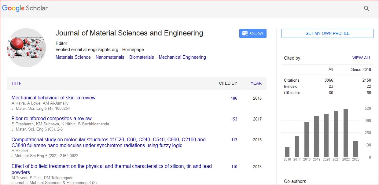
Journal of Material Sciences & Engineering received 3677 citations as per Google Scholar report


 Spanish
  Chinese
  Russian
  German
  French
  Japanese
  Portuguese
  Hindi
Hindi 