Sheikh A Akbar
Posters-Accepted Abstracts: J Material Sci Eng
Recent work in the author’s laboratory has led to the development of simple processes for the fabrication of ordered and
self-assembled nanostructures by exploiting intrinsic mate-rial properties that are inexpensive, highly scalable and do
not require use of lithography. These processes can be classified as “oxide nanostructures by materials design”. One process
creates nanofiber arrays of single crystal TiO2 by gas phase reaction in a H2/N2 environment. As oxygen from TiO2 is taken
out as H2O (g), Ti diffuses from the surface to the bulk resulting in fibers oriented along the <001> direction. Work on single
crystal TiO2 shows that on Au-catalyzed (001) surface, oriented nano-fibers can be grown with <001> and <110> alignments
using H2/N2 heat treatment. The same gas heat treatment was also used to grow nanofibers on polycrystalline SnO2 in regions
of the sample coated with gold, showing directional growth on grains with crystal facets. We have also devel-oped a process
to create nanofibers of TiO2 on Ti metal and Ti alloys via oxidation under a limited supply of oxygen (~10s of ppm). Lately,
we have succeeded in converting the 1-D TiO2 nano-fiber grown by thermal oxidation to nano-dendritic titanates by a hydrothermal
treatment. The conversion of TiO2 to barium (and other) titanates is a path to syn-thesizing materials in a different
class of functionality because of their piezoelectric and ferroelectric responses. We developed yet another interesting nanostructure
(nanoislands and nanobars) during thermal annealing of an oxide (GDC) on top of another oxide (YSZ) substrate
that self-assembles along the softest elastic direction of the substrate. What is common about these structures is that they are
fabricated without the use of lith-ographic techniques and involves simple processes such as gas-phase reactions and stressdriven
process. These nano-structures can be used as platforms for chemical sensing, photo catalysis, electro emission and
biomedical applications. Preliminary results of some of these applications are presented.
Sheikh A. Akbar is a Professor of Materials Science and Engineering and Founder of the National Science Foundation (NSF) Center for Industrial Sensors and
Measurements (CISM) at The Ohio State University in Columbus, OH, USA. His recent work deals with synthesis-microstructure-property relations of ceramic bulk,
thin-film and nano-structures. Dr. Akbar was the Chair of the 12th International Conference on Chemical Sensors (IMCS-12) held in 2008. This meeting was attended
by 330 participants from more than 30 countries. His sensors received three (3) R&D 100 Awards as part of the 100 best inventions of 2007 and 2005 selected by
R&D Magazine and 2005 NASA TGIR (turning goal into reality) award. Dr. Akbar is the recipient of the 2012 Electrochemical Society Sensor Division Outstanding
Achievement Award, the 2002 Tan Chin Tuan Fellow of Nanyang Technological University in Singapore, and the 2001 Fulrath Award and the 2002 W.E. Cramer Award
of the American Ceramic Society. He was elected a Fellow of the American Ceramic Society in 2001. He also received the 1993 B.F. Goodrich Col-legiate Inventors
Award for the development of a rugged and durable CO/H2 sensor; one of three national awards. Dr. Akbar served on the International Advisory Committee of CIMTEC
conferences, Steering Committee of the International Conference on Engineer-ing Education (ICEE), Technical Steering Committee of the US-DOE Sensor and Controls
Program, and the Steering Committee of the US-Japan Conference on Sensor Sys-tems for the 21st Century. He has co-organized sensor symposia for the
American Ceramic Society, the Electrochemical Society, ICMAT (Singapore) and ICC3 (Japan). Dr. Akbar has co-edited 2 books on sensors. In 2003, he served as the
Guest Editor for two special sections of the Journal of Materials Science, “Chemical Sensors for Pollution Monitoring and Control” and “Chemical and Bioceramics.”
Recently, he was the Principal Editor of special issues entitled, “Nano-structured Ceramic Oxides: Challenges and Opportunities” and “Energy and Environment: Role of
Advanced Materials” published by the American Scientific Publisher in 2011 and 2014, respectively. He is also the Guest Editor of a special issue entitled, “Sensing at
the Nano-scale: Chemical and Biosensing” published in 2012 in Sensors. Dr. Akbar is on the Editorial Board of the Journal of Nanoengineering and Nanomanufacturing,
Materials Focus, Ceramics International, Journal of Nanomaterials and Sensor Letters. He has published more than 200 technical papers and holds 8 patents.
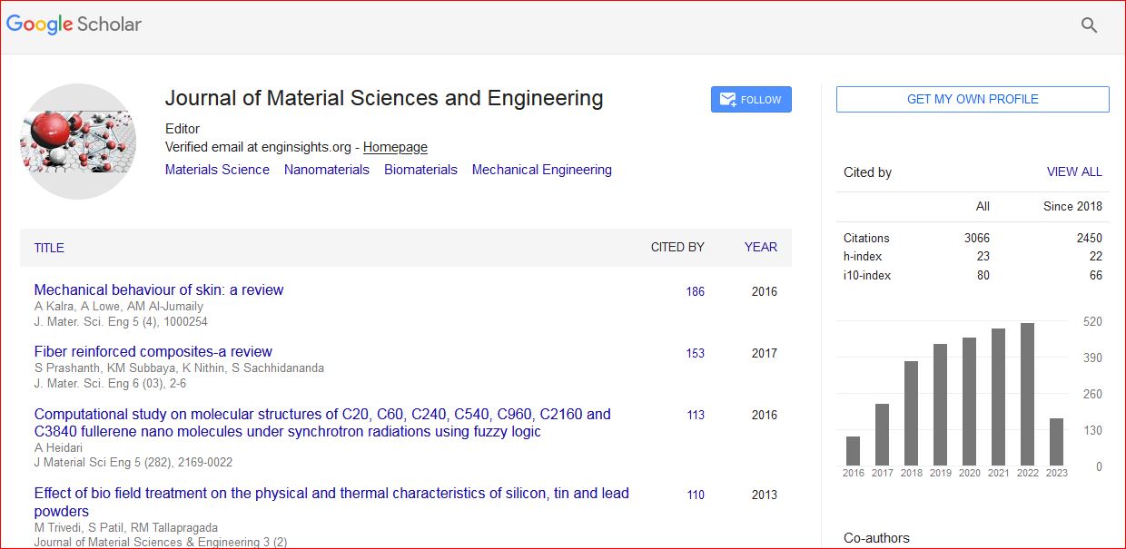
Journal of Material Sciences & Engineering received 3677 citations as per Google Scholar report


 Spanish
  Chinese
  Russian
  German
  French
  Japanese
  Portuguese
  Hindi
Hindi 