 |
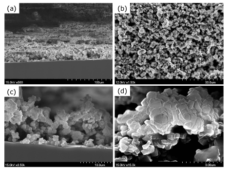
| Figure 5: High-resolution field emission SEM images of ZSM-5(10)/Tenax TA on a Si wafer: (a) a cross-sectional image (film thickness, approximately 30 μm), (b) highly uniform and porous surface of the film, (c) and (d) images after coating the Tenax TA polymeric phase that is penetrated into the film from the top surface of ZSM-5 layer to the bottom (irregular shape agglomerates between cubic ZSM-5 crystals are supposed to be the polymer). |