


 10 / 15

Volume 4, Issue 2 (Suppl)
J Laser Opt Photonics, an open access journal
ISSN: 2469-410X
Page 44
conference
series
.com
JOINT EVENT
July 31- August 02, 2017 Milan, Italy
&
6
th
International Conference on Photonics
7
th
International Conference on Laser Optics
Nanostructured GaN light-emitting diodes on unusual substrates and blue light enhancement by
surface plasmon resonance
T
here have been significant recent developments in the growth of single crystal gallium nitride (GaN) on unconventional
templates for large-area blue or green light-emitting diodes (LEDs) which, together with layer transfer onto foreign
substrates, can enable flexible and stretchable lighting applications. Here, the heteroepitaxial growth of GaN on amorphous
and single-crystal substrates employing various interlayers and nucleation layers is discussed, as well as the use of weak
interfaces for layer-transfer onto foreign substrates. Layer-transfer techniques with various interlayers are also discussed. These
heteroepitaxial GaN growth and layer-transfer technologies are expected to lead to new lighting and display devices with high
efficiency and full-color tunability, which are suitable for large-area, stretchable display and lighting applications. We shall also
discuss blue light enhancement in CdS/ZnS quantum dots using surface plasmon resonance to achieve near-unity quantum
yield. Finally, nanostructured GaN-based LEDs for white light generation will be reviewed.
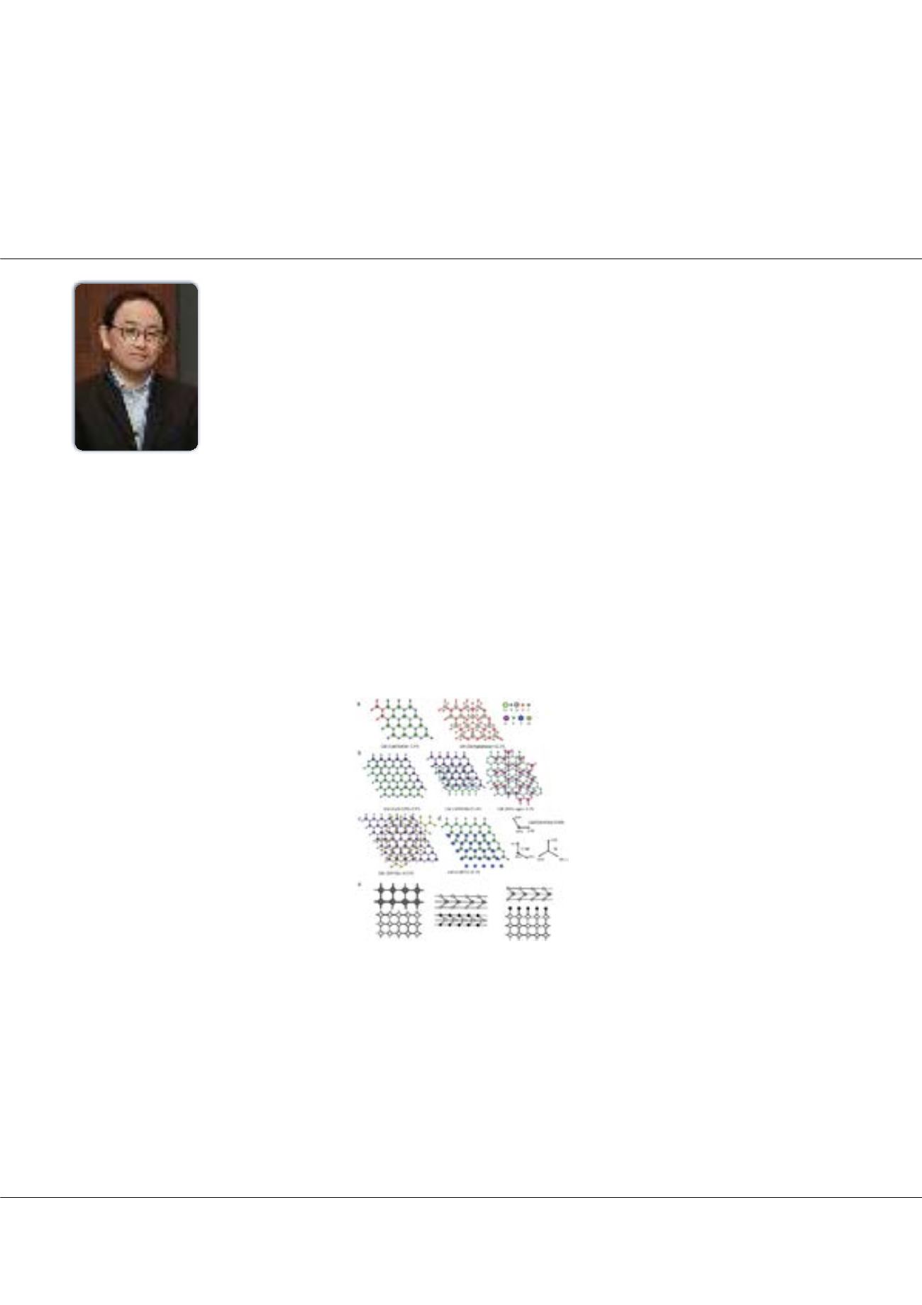
Figure1:
Atomic arrangement of various hetero-epitaxial interfaces for different multilayer structures: a) GaN/ZnO (NL)/graphite (IL/SB): (left) GaN/ZnO and (right) ZnO/
graphene. b) GaN/AlN (NL)/BN (IL)/sapphire (SB): (left) GaN/AlN, (center) AlN/BN, and (right) BN/sapphire. c) GaN/Ti (IL)/glass (SB): GaN/Ti. d) GaN/AlN (IL)/Si (SB):
AlN/Si. e) Interfaces connected by (left) dangling bonds (3D on 3D), (center) van der Waals gap (2D on 2D), and (right) quasi van der Waals gap (2D on dangling-bond
passivated 3D).
Biography
Jun Hee Choi received his PhD in Materials Science and Engineering from Seoul National University in 2012. He is currently a Research Master and Research Staff
Member of the Device and System Research Center at Samsung Advanced Institute of Technology, Samsung Electronics. He has published more than 45 papers in
SCI journals, more than 20 conference papers, and more than 50 US patents. His research includes GaN-based optoelectronics on unconventional substrates, and low
dimensional electronics based on quantum dots, ZnO nanorods, and graphene.
joonie.choi@samsung.comJun Hee Choi
Samsung Electronics, South Korea
Jun Hee Choi, J Laser Opt Photonics 2017, 4:2(Suppl)
DOI: 10.4172/2469-410X-C1-010