


 11 / 36

Page 37
Notes:
conferenceseries
.com
Joint Conference
July 17-18, 2017 Chicago, USA
International Conference on
DIAMOND AND CARBON MATERIALS & GRAPHENE AND SEMICONDUCTORS
Volume 6, Issue 6 (Suppl)
J Material Sci Eng, an open access journal
ISSN: 2169-0022
Diamond and Carbon 2017 & Graphene 2017
July 17-18, 2017
The solution-based sorting and assembly of single-walled carbon nanotubes for transistors and
pressure sensors
Steve Park
Korea Advanced Institute of Science and Technology, South Korea
S
ingle-walled carbon nanotubes (SWNTs) are an ideal channel material for next generation sub-10 nm gate-length transistors
due to their ultra-thin body and high carrier transport properties. In addition, due to their high mechanical flexibility,
SWNTs are an ideal candidate for flexible and stretchable sensors and electronics. To use SWNTs as channel material in
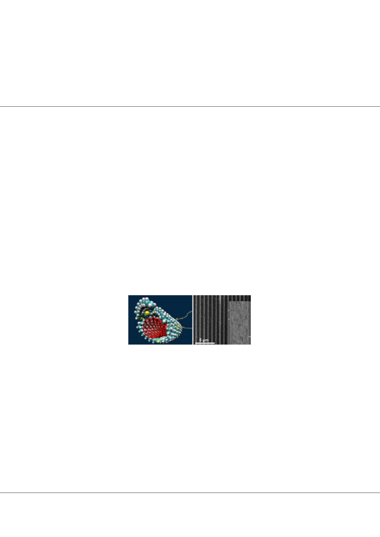
transistors, 1) semiconducting SWNTs must be fully separated from metallic SWNTs and 2) densely aligned over a large
area, in a facile and scalable manner. To address the former, we have investigated solution-based sorting of SWNTs using
various conjugated polymers. With proper design of conjugated polymers, certain diameter range of the semiconducting
SWNTs was selectively dispersed with high efficiency. To address the latter, we have developed solution-shearing technique to
densely align SWNTs over a large area, with density as high as 200 SWNTs/μm. On-current density was improved by an order
of magnitude over that of random network; however, with higher packing density, loss of electrostatic control was evident.
These observations shed light on the behavior of aligned SWNT films and suggest possible approaches to further improve
the electrical properties of SWNT-based transistors. We have also developed a stretchable capacitive tactile sensor based on
carbon nanotube electrodes. By buckling the carbon nanotubes into 'nanosprings,' high degree of stretchability up to 100% was
attained. As the dielectric layer, we have implemented an air gap and a porous PDMS layer. The air gap enabled high sensitivity
of 0.7 kPa^-1 in the low pressure regime (<1 kPa), while the porous PDMS layer enabled better pressure sensitivity in the tens
of kPa regime. In addition, by simultaneously detecting the change in capacitance and the resistance of the top and bottom
electrodes, various tactile inputs such as normal pressure, bending, and lateral strain was differentiated.
Biography
Steve Park received his dual Bachelor’s degree in Materials Science and Engineering and Physics with great distinction from the University of Illinois at Urbana-
Champaign and Knox College. He then worked as a technical staff for NanoInk Inc., developing commercial applications of dip-pen nanolithography. He then
received his Master of Science and PhD from Stanford University in Materials Science and Engineering under the Prof. Zhenan Bao, researching on carbon
nanotube and organic-based electronics. He then conducted his Post-doctoral work at Columbia University in the Electrical Engineering and Biomedical Engineering
Department, working on piezoelectric polymer-based implantable devices.
stevepark@kaist.ac.krSteve Park, J Material Sci Eng 2017, 6:6(Suppl)
DOI: 10.4172/2169-0022-C1-076