


 12 / 36

Page 39
Notes:
conferenceseries
.com
Joint Conference
July 17-18, 2017 Chicago, USA
International Conference on
DIAMOND AND CARBON MATERIALS & GRAPHENE AND SEMICONDUCTORS
Volume 6, Issue 6 (Suppl)
J Material Sci Eng, an open access journal
ISSN: 2169-0022
Diamond and Carbon 2017 & Graphene 2017
July 17-18, 2017
Graphene/fluorinated graphene systems for a wide spectrum of applications
Irina V Antonova
Institute of Semiconductor Physics, Russia
I
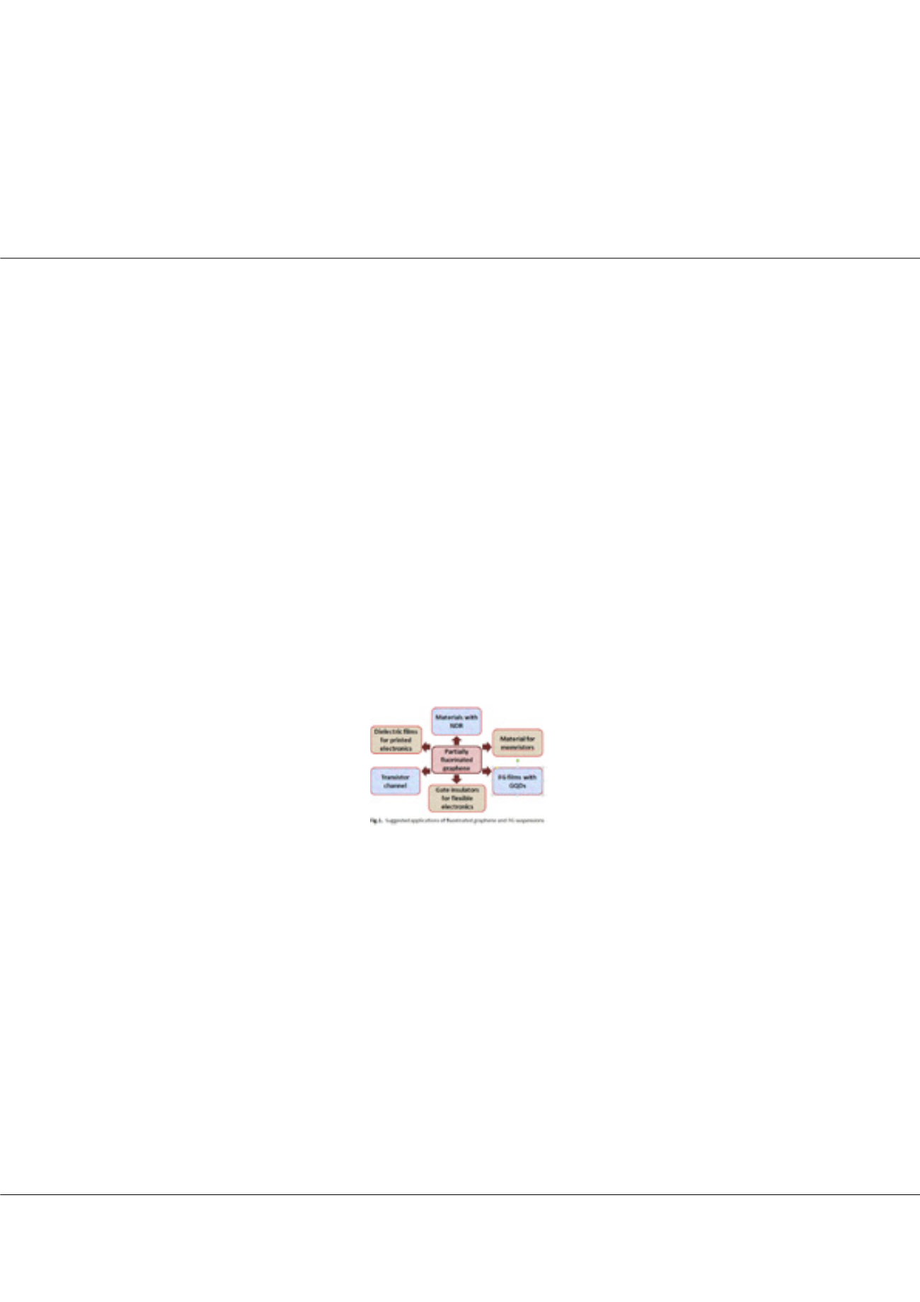
n the report we consider the properties of partially fluorinated graphene (FG) created with the use of a simple fluorination
method based on the treatment in an aqueous solution of hydrofluoric acid. FG films can be formed from CVD grown
graphene and a graphene suspension. A possibility to control a size of graphene flakes in a suspension in the course of their
fluorination was also demonstrated. The possibility to create the FG films with arrays of graphene quantum dots (GQDs) is
revealed. The spectrum of quantum confinement levels for GQDs in a fluorinated matrix and a charge relaxation time from
GQDs are determined with the use of charge transient deep level spectroscopy. The time of GQD recharging can be controlled
by means of GQD thickness variation or daylight assistance. This finding makes films with GQDs promising for flash memory
applications. Fluorination of domain boundaries leads to a strong current modulation by gate voltage with an ON/OFF relation
~105 (the property important for field-effect transistors). The negative differential resistance (NDR) and a step-like increase
in the current are found for films created from the fluorinated graphene suspension. The NDR resulting from the formation of
a potential barrier system in the film is observed for a relatively low fluorination degree. The observation of NDR in FG films
widens the range of possible applications. A stable resistive switching effect is detected in films created from the FG suspension.
The origin of resistive switching was found to connect with the appearance of traps with energy 0.08 eV and the recharging
time lower than 700 ns. The charges in metal–insulator–semiconductor structures with FG dielectric layer have been estimated
as the ultra-low values of (0.5–2) x1010 cm-2. Suspensions of fluorinated graphene with nanometer size flakes are of interest
for the development of 2D ink-jet printing technologies and the production of thermally and chemically stable dielectric films
for nanoelectronics on rigid and flexible substrates.
Biography
Irina V Antonova graduated from Department of Physics and Engineering, Novosibirsk State Technical University in 1979. Since 1981, she has been working in the
Institute of Semiconductor Physics, Siberian Branch of the Russian Academy of Science. Presently, she occupies a leading Researcher Position at the Institute of
Semiconductor Physics and heads a group of researchers who deal with investigation of graphene and its derivatives. Her activity was connected with transport
and recharging phenomena in nanocomposite layers (Si, Ge nanocrystals in dielectric matrix), and localized states in heterostructures (SOI, quantum wells
and quantum dots), high-pressure-related effects and surface passivation phenomena. The scope of her current research includes chemical functionalization of
graphene, fabrication of graphene-based heterostructures and arrays of graphene quantum dots embedded in a fluorographene matrix, transport and recharging
phenomena in nanocomposite layers. She has above 240 papers.
antonova@isp.nsc.ruIrina V Antonova, J Material Sci Eng 2017, 6:6(Suppl)
DOI: 10.4172/2169-0022-C1-076