Morphological and Structural Investigation of Chemically Synthesized Copper Indium diSelenide (CIS) Ternary Thin Films
Received: 19-Sep-2018 / Accepted Date: 12-Oct-2018 / Published Date: 19-Oct-2018
Abstract
Ternary thin films of Copper Indium di-Selenide (CIS) has been prepared on glass substrates at 85°C by Chemical Bath Deposition technique and the morphological and structural properties were investigated. The deposition was based on the reaction between aqueous solution of CuCl2.2H2O, InCl3.4H2O and Na2SeSO3, in an alkaline medium of NH3(aq) withTEA and EDTA as complexing agents. One of the films samples labeled as-deposited and the other, annealed at 450°C in an electric furnace. The crystalline nature of the CIS showed that the as-deposited films were amorphous in nature meanwhile the annealed films were crystalline in nature which showed the effect of annealing on the samples. The SEM micrograph of the thin films showed a coarse distributed structure and finely distributed structure for as-deposited and annealed films respectively.
Keywords: CIS; Ternary; Thin films; Chemical bath; Morphological; Structural
Introduction
Chemical Bath Deposition (CBD) refers to a typical synthesis employing mild conditions [1]. The technique of Chemical Bath Deposition involves the controlled precipitation of a compound from a solution on a suitable substrate. This technique offers many advantages over the more established vapour phase routes to semiconducting thin films, such as CVD (Chemical Vapour Deposition), MBE (Molecular Beam Epitaxy) and spray pyrolysis. In this preparation technique it is possible to control the film thickness and composition by varying the solution pH, temperature and reagent concentration. The ability of CBD to coat large areas in a reproducible and low cost process is one added attraction of this method. The first report of CBD was in 1884 for the preparation of PbS [1]. Today a wide range of chalcogenides (e.g. CdS, ZnSe, MnS) and chalcopyrite materials (e.g. Culns, and CulnSe2) have been prepared using this method. In chemical bath deposition process, precipitation of the solid phase occurs due to the super saturation in the reaction bath. At a given temperature when ionic product of reactants exceeds the solubility product, precipitation occurs. Whereas if the ionic product is less than the solubility product, then the solid phase produced will dissolve back to the solution resulting in no net precipitation. This forms the basic principle behind any chemical deposition process. In other words, the principle of CBD technique is to control the chemical reaction so as to effect the deposition of a thin film by precipitation.
Recent years have witnessed intensive research in the field of preparation and characterization of thin film chalcogenides. These semiconductor compounds find numerous applications in electronic and electro-optical devices. In the present century, thin film heterojunction solar cells are going to play an important role as low cost, large area and high efficiency devices in solar energy conversion. Today there are well established n-type semiconducting films such as SnO, InO, InSnO and CdS which act as window material when deposited on p-type semiconductors, giving rise to various types of heterojunctions. On the contrary, there are only few thin films showing p-type conduction. Cuprous chalcogenide binary films such as CuS, CuSe and CuTe are typically p-type and highly conductive. Among these, copper selenide is an interesting metal chalcogenide semiconductor with a wide range of stoichiometric compositions and also with various crystallographic forms for each of these compositions. The well-known forms of these compounds include CuSe, Cu2Se3 and Cu5Se8, though other compositions for CuSe were also reported by Hamakawa [2]. There are also many crystallographic forms of copper selenide thin films such as monoclinic, orthorhombic, cubic, tetragonal and hexagonal. It is also reported that CuSe has a hexagonal structure at room temperature and undergoes transition to an orthorhombic structure at 48°C and back to a hexagonal structure at 120°C [3-5]. This study looked into the structure and compositions of CuSe when doped with a controlled amount of Indium content.
Materials and Method
The starting chemicals used in this study were copper (II) chloride dihydrate (CuCl2.H2O) as the source of Cu2+ and Triethanolamine (TEA) as a complexing agent, sodiumselenophite (Na2SeSO3) as a source of selenium ion (Se2-) and Indium (III) chloride tetrahydrate (InCl3.4H2O) as a source of indium ion (In3+) whereas Ethylene Ditetra Amine Acid (EDTA) as a complexing agent for In2+ in the reaction mixture of both. Ammonia (NH3) was used to adjust the pH of the solution. The sodium selenosulphite was prepared by refluxing 9.0 g of selenium power with approximately 15.0 g of anhydrous sodium sulphite (Na2SO3) in 200 mL of distilled water for 6 h at 80°C thereby making 0.2 M of Na2SeSO3.
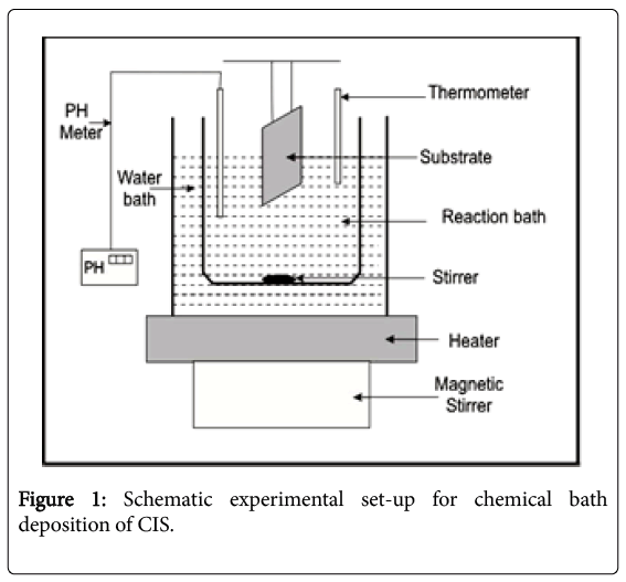
CIS thin films were synthesized on glass substrates by CBD technique at 85°C. Prior to the growth, the glass substrates were degreased in HCl for 24 h, washed with detergent, rinsed with distilled water and dried in air. The deposition of CIS thin film was based on the reaction between aqueous solution of CuCl2.2H2O), InCl3.4H2O and Na2SeSO3, in an alkaline medium of NH3(aq) and TEA and EDTA as complexing agents. For deposition, three reaction baths S1, S2, and S3 (100 mL beaker each) were used. 10 mL of CuCl2.2H2O were measured into a 50 mL beaker using burette, 5 mL of TEA were added to it, InCl3.4H2O were measured into a 50 mL beaker using burette 5 mL of 0.5 mol trisodium citrate were then added. 20 mL Na2SeSO3, 20 mL NH3(aq) were added to the solution. The mixture was topped to 90 mL level by addition of distilled water and stirred gently to ensure uniformity of the mixture. Copper (II) chloride dihydrate (CuCl2.2H2O), Indium (III) chloride tetrahydrate (InCl3.4H2O) and sodium selenosulphite (Na2SeSO3) were the sources of Cu2+, In3+ and Se2- respectively. The deposition process was carried out at different deposition times of 3, 6, 9, 12 and 15 h in order to determine the optimum condition for the deposition of CIS thin film. The experiment was conducted at 85°C temperature. Four cleaned glass substrates were vertically immersed into the chemical baths with the help of a suitable designed substrate holder as shown in Figure 1. After the deposition, the substrates were removed from the mixture and allowed to dry under ambient condition. One of the films samples was labelled asdeposited and the other two samples were annealed at 200°C and 450°C in an electric furnace respectively. The various deposition temperatures and the pH (11.5-11.3) were monitored with Mettler Toledo AG 8603 pH meter. The substrates were removed, rinsed in distilled water and dried in open air at room temperature and kept. Table 1 shows the chemical bath compositions for the deposition of the thin films.
| Baths | Cu | In | Se | pH |
|---|---|---|---|---|
| Concentration (M) | ||||
| S1 | 0.3 | 0.1 | 0.2 | 11.5 |
| S2 | 0.3 | 0.2 | 0.2 | 11.4 |
| S3 | 0.3 | 0.3 | 0.2 | 11.3 |
Table 1: Chemical bath compositions for the deposition of CIS thin films.
Results and Discussion
Results
The crystallographic structure of CIS was analyzed with an X-ray diffractometer. Scanning Electron Micrograph (SEM) measurements were conducted using SEM machine (Inspect X50). The thickness, composition of layers and coating and chemical composition analysis of the thin films were determined using X-ray Fluorescent (XRF) spectroscopy (Sky Ray Explorer). The Structural analysis of the CIS thin films was done by XRD machine (Shimadzu 6000).
Discussion
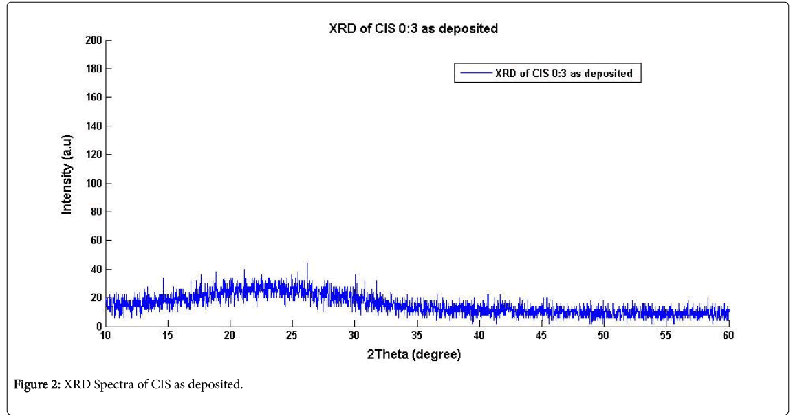
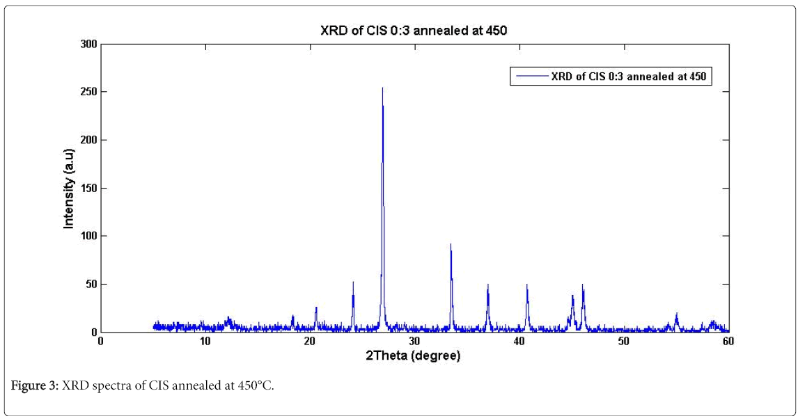
Table 1 shows varied compositions for the films in different baths, but similar results were obtained for these varied compositional baths which indicated that bath S1 had the optimized composition of the deposited films. Figures 2 and 3 show the XRD patterns for the asdeposited and annealed CIS thin films of thickness 0.2 nm which was obtained from a non-destructive Surface Profiler. One technique to measure film thickness is by scanning white light interferometry [6]. The reference surface of the interferometer is scanned vertically to acquire white light interferogram. A large number of frames were recorded and processed to get the three dimensional profile and thickness of the sample. Many different types of measurement techniques also used only for surface profiling [7]. Reflectometry is long available technique for measurement of the film thickness [8,9]. It measures reflectance for different wavelength to calculate thickness. This technique can only determine the film thickness and it is a point detection technique. Recently, reflectometry and spectrally resolved white light interferometry were combined for measurement of film thickness and surface profile using Linnik interferometer [10].
The XRD patterns revealed amorphous nature of the films with a broad band at indistinct diffraction peaks. This amorphous structure was found to be unstable as thermal annealing subsequently leads to crystallization in the film [11]. The thermal annealing of the asdeposited thin films at 200°C and 450°C were performed for 50 min and 180 min respectively which resulted to no visible effect (result similar to that of as-deposited film) on the former whereas resulted to a crystallization with distinct peaks in the latter. This indicates that at the temperature of 450°C, the crystallites in the samples have been reordered thereby improving the crystallinity of the material. In this way, the films become free of probable defects generated during the deposition. Distinct peaks for the CIS annealed film were identified at 173 intensity count with 26.98° 2θ corresponding to 0.4750 Full Width Half Maximum (FWHM) orientation planes. The respective positions of the peaks were identified in accordance with the JCPDS standard data. The intensity count of the diffraction lines corresponding to 39.56° 2θ is better resolved. This is in consistence with the work of Ahmed who reported that occasionally, the formation of a more relaxed structure could be achieved in the as-deposited films [12,13]. The crystalline size of the CIS was 472.68-31883.35 nm.
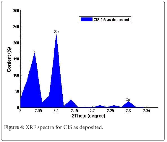
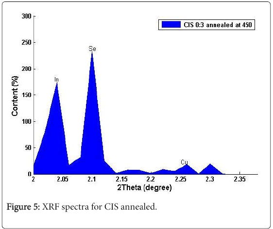
Figures 4 and 5 showed the weight percent composition (measurement accuracy of ± 2%) for a range of total weight of deposit for different samples of CIS thin films. The apparent measurement error could be due to the fact that the sample area for analysis was restricted and the calibration conditions and those of the analyses were not identical. Energy dispersive X-ray fluorescence analysis confirmed the presence of Cu (4.4)%, In (37.4)% and Se (50.6)%, with 2.30°, 2.05° and 2.10° of 2θ values respectively, which shows that the CIS deposited is nearly stoichiometry. The results from XRF indicated that the asgrown films were slightly deficient in selenium and complete absence of copper was found in films deposited at source temperatures below 1100°C. These results make Chemical Bath Deposition (CBD) more preferable to other methods for its large areas of coating thereby revealing sufficiently the elemental compositions in the deposited films.
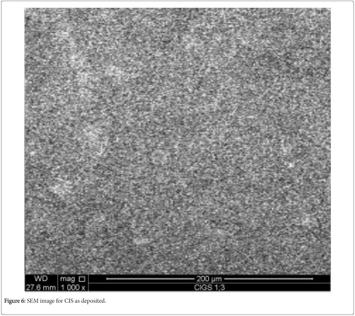
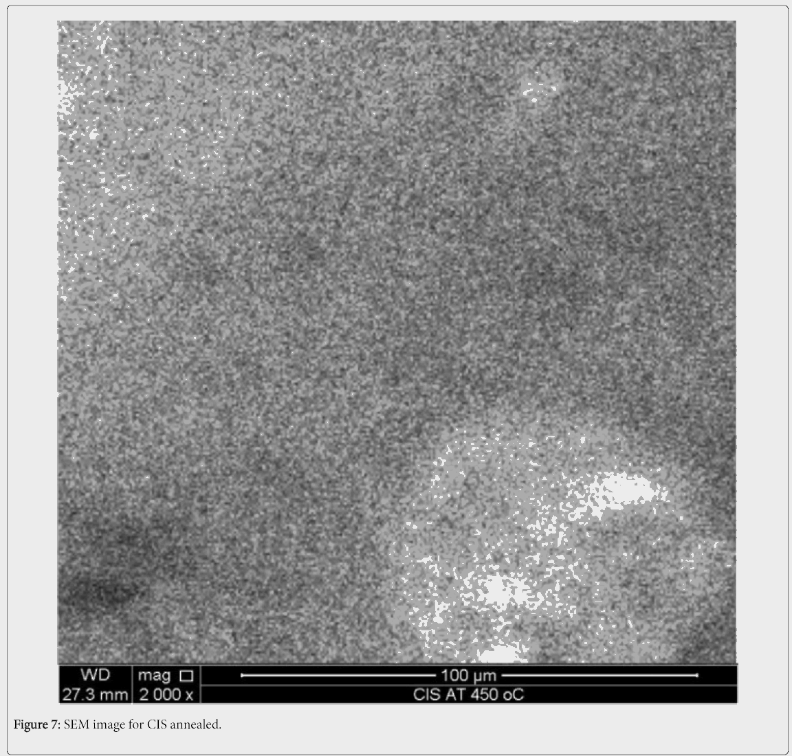
The scanning electron micrographs of the CIS samples prepared under optimized deposition conditions are shown in Figures 6 and 7. The grain size of the as-deposited sample was estimated from the SEM micrographs and was found to be 100 μm and same size was observed for the annealed sample with magnification of 500. This agrees with the report of Babatunde, who deposited ZnSe on SLG using thermal evaporation technique [14]. The SEM micrograph of the thin film showed a denser sponge-like structure. By considering the deposition conditions, it can be concluded that the in-situ annealing resulted in a more relaxed and denser structure. No clear difference between the films as deposited and annealed at 450°C temperature. This is similar to the report of Dr. Stefan [15].
Conclusion
CIS ternary thin films have been deposited successfully on microscopic glass substrates using Chemical Bath Deposition (CBD) technique. The structural, compositional and morphological properties of the as-deposited and annealed thin films at 450°C temperature have been studied. The crystalline nature of the CIS showed that the asdeposited films were amorphous in nature meanwhile the annealed films were crystalline in nature which showed the effect of annealing on the samples. The XRF analysis confirmed the presence of CIS and other elements in the deposited thin films. The SEM micrograph of the CIS thin films showed a coarse distributed structure and finely distributed structure for as-deposited and annealed films respectively.
References
- Lakshmi M (2001) Studies on chemical bath deposited semiconducting copper selenide and iron sulfide thin films useful for photovoltaic applications. PhD Thesis. Cochin University of Science and Technology, India.
- Hamakawa JA (2004) Background and motivation for thin-film solar-cell development. In: Hamakawa Y. (eds) Thin-Film Solar Cells. Springer Series in Photonics 13: 1-2.
- Lakshmi M, Bindu K, Bini S, Vijayakumar KP, Kartha CS, et al. (2001) Reversible Cu2−xSe↔Cu3Se2 phase transformation in copper selenide thin films prepared by chemical bath deposition. Thin Solid Films 386: 127-132.
- Haram SK, Santhanam KSV, Numannspallart M, Levyclement C (1992) Electroless deposition on copper substrates and characterization of thin films of copper (I) selenide. Mater Res Soc Bull 27: 1185-1191.
- Gracia VM, Nair PK, Nair MTS (1999) Copper selenide thin films by chemical bath deposition. J Cryst Growth 203: 113-124.
- Kim SW, Kim GH (1999) Thickness profile measurement of transparent thin-film layers by white-light scanning interferometry. Appl Opt 38: 5968-5973.
- Yoo HK, Lee SW, Kang DK, Kim TJ, Gweon DG, et al. (2006) Confocal scanning microscopy: A high-resolution nondestructive surface profiler. Int J Precis Eng Man 7: 3-7.
- Tompkins HG, McGahan WA (1999) Spectroscopic Ellipsometry and reflectometry: A user’s guide. Wiley Interscience.
- Rosencwaig A, Opsal J, Willenborg DL, Kelso SM, Fanton JT (1992) Beam profile reflectometry: A technique for dielectric film measurements. Appl Phys Lett 60: 1301-1303.
- Ghim YS, Kim SW (2007) Fast, precise, tomographic measurements of thin films. Appl Phys Lett 91: 91903.
- Fang G, Liu Z, Yao KL (2001) Fabrication and characterization of electrochromic nanocrystalline WO3/Si (111) thin films for infrared emittance modulation applications. J Phys D 34: 15.
- Ahmed E (1995) Growth and characterisation of Cu(In,Ga)Se2 thin films for solar cell applications. PhD Thesis, University of Salford, UK.
- Ahmed E, Zegadi J, Hill KD, Pilkington HF, Tomlinson Y, et al. (1998) Flexible and light weight copper indium diselenide solar cells on polyimide substrates. Sol Energy Mater Sol Cells 43: 93-98.
- Babatunde RA (2017) Synthesis and characterization of ZnTe and ZnSe Thin films as window layers for heterojunction solar cell deposited by thermal vaccum evaporation. MSc Dissertation, Olabisi Onabanjo University, Nigeria.
- Talu S (2013) Characterization of surface roughness of unworn hydrogel contact lenses at a nanometric scale using methods of modern metrology. Polym Eng Sci 53: 2141-2150.
Citation: Adeniji QA, Odunaike K (2018) Morphological and Structural Investigation of Chemically Synthesized Copper Indium diSelenide (CIS) Ternary Thin Films. J Mater Sci Nanomater 2: 108.
Copyright: © 2018 Adeniji QA, et al. This is an open-access article distributed under the terms of the Creative Commons Attribution License, which permits unrestricted use, distribution, and reproduction in any medium, provided the original author and source are credited.
Select your language of interest to view the total content in your interested language
Share This Article
Recommended Journals
Open Access Journals
Article Usage
- Total views: 4077
- [From(publication date): 0-2018 - Dec 19, 2025]
- Breakdown by view type
- HTML page views: 3136
- PDF downloads: 941

