A Review on Theoretical Studies of Optical and Electrical Parameters Values of Thin films
Received: 03-Oct-2017 / Accepted Date: 07-Oct-2017 / Published Date: 15-Dec-2017 DOI: 10.4172/2168-9806.1000177
Abstract
This article provides an overview of research on nanoparticles quantum confinement processing of nanoparticles and processing applications in theoretical concepts of optical and electrical studies. The main text of this review is organized into two sections. Section 1 discusses the use of optical methods for the applications of nanoparticles and its model exciton properties of nanostructured particles and in section 2 discusses for dispersion of agglomerated nanoparticles and its various equations for all, such as photo luminescent and transparent conductive materials. These studies explain the theoretical equations of both nanoparticles and thin film.
Keywords: Exciton; Luminescent; Bohr radius; Complex impedence spectroscopy (CIS)
Introduction
Miniaturisation leads to devices which are faster, more versatile, more efficient, less power consuming and cheaper. Nanotechnology is the logical extension of MEMS (Microelectromechanical systems). However, its scope is immense and many opine that it is the onset of the second industrial revolution. It is going to affect the human society in a way more radical than the earlier innovations in science and technology. The present chapter is intended to provide the student a glimpse of the revolution that is underway. Quantum-size effects of Wannier excitons in semiconductor mocrocrystals have been a subject of extensive studies in recent years. A wide variety of materials have been grown as microcrystals in glasses, in alkali-halide crystals, in liquids, and also in vacuum. The size quantization effect is most directly detected as the high-energy shift of the inter band absorption or luminescence peak in these materials. In addition to the interest in the basic properties of the quasiparticles confined in the three-dimension quantum well, the potential applicability to the ultrafast nonlinear optical devices seems to have motivated some of the recent investigations.
Fundamentals of quantum confinement of NPs
From the theoretical point of view, the ground-state property of an electron and a hole confined in a micro crystal poses a fundamental problem of quantum mechanics: the competition between the attractive two-body force and the one-body force exerted at the well boundary. It can be readily inferred that there are two limiting situations according to the ratio of the characteristic length R indicating the size of the microcrystal to the effective Bohr radius  of the exciton in the bulk material. In the limit
  , the character of the exciton as a quasiparticle is conserved well while the translational degrees of freedom are confined with little energy increment (the regime of the exciton confinement). In the opposite limit
  , the electron and the hole should occupy primarily the individual lowest eignstae of the quantum well with relatively little spatial correlation (the regime of the individual particle confinement). One of the central problems is, therefore, to make clear how the motional state of the electron-hole system changes as the ratio
  changes continuously and to give of the lowest state as a function of .
Brus derived an expression of the energy of the lowest eigenstate in this limit. On the other hand, the analysis of the weak confinement limit is rather a difficult task because it is not known what to choose as the zeroth-order approximation for the wave function which satisfies the boundary condition [1]. Efors an Efors asserted that the amount of the energy increment in this limit is given just by the value corresponding to that of a single point particle with the mass equal to the total mass of the exciton [2]. The present author carried out a simple variational calculation of the ground-state energy of the electron-hole system in a spherical quantum well. The proposed trial wave function, which contains only one parameter, bridges the above-mentioned two limiting cases and naturally covers the whole range of , where R is the radius of the sphere in this case. It was pointed out that the transition between the two regimes occurs at around  ≅ 2 ~ 3 continuously but rather abruptly.
In the present paper, we study the quantum-size effects of the electron and the hole in a spherical well to the full extent both analytically and numerically, A new type of the variational calculation is developed, which, we believe, gives a very accurate approximation to the exact eignenergy of the ground state and of the low-lying excited states in a wide range of parameter values. In practice, however, the ground-state energy but also the level structure of the expressed far better by a formula which takes into account the finiteness of the exciton radius. Not only the ground-state energy but also the level structure of the excited states and the distribution of the oscillator strength for the optical transition are investigated. It will be shown that because of the broken symmetry of the translational degrees of freedom, the optical absorption spectrum of the weakly confined exciton has side bands closely lying above the 1s peak and the whole Rydberg [3] series structure gradually changes into the series of well-isolated peaks peculiar to the strong confinement as R / a* becomes small [4].
Let us consider an electron and a whole confinement in a microcrystal of spherical shape with the radius R. The microcrystal is approximation by an isotropic continuous medium with the dielectric constant k. We neglect the effect of the polarization charge induced at the surface for simplicity. It is assumed that the electron and the hole are completely confined in the well by the infinite potential barrier. Our main concern here is to clarify the essential features of the problem by a simplified model, which will serves as a starting point of the analysis in real materials.
The Hamiltonian is given by
 (1)
(1)
Where ri, pi and mi are the coordinate, the momentum, and the mass for the electron (i=e) and the hole (i=h), respectively.
The total mass M=me+mh and the reduced mass  will also be used hereafter. The boundary condition is that the wave function Ψ should vanish at
The rotational invariance around an arbitrary axis allows us to separate out three angle variables and we are left with only three independent variables relevant to the Schrodinger equation. In carrying out the numerical calculation, the crucial step here is to choose the Hylleraas coordinates,  for these variables.
The Euler angles determining the plane on which re and rh lie can be chosen as the remaining three variables. The eigenstates of the Hamiltonian are classified in accordance with the total angular momentum J, the magnetic quantum number M, and the one additional quantum number k for the vector spherical harmonics. In each subspace of (J, M, k), the Schrodinger equation can be explicitly written down. Throughout the present work, we are solely concerned with the s-like subspace (J=0) only to which the inter band transition is possible in the direct allowed semiconductors. The Hamiltonian is then greatly simplified as given by the previous paper.
If one adopts the effective Rydberg energy  for the unit of the energy and the effective Bohr radius
  for the unit of the length, the normalized ground-state energy
  can be written as a function of two independent dimensionless parameters as
ε=ε(σ, ρ), (2)
where σ=mh/me is the mass ratio and ρ ≡ . Since ε(1/σ, ρ)=ε(σ, ρ), we assume σ≥1 hereafter. First of all, the following inequality can be easily proven by using Hellmann-Feynman’s theorem,
∂ε (σ ,ρ ) / ∂σ < 0 forσ ≥1 (3)
Which means that the ground-state energy is a decreasing function of the total mass for a fixed value of the reduced mass and well radius? The asymptotically exact solution for ε(σ, ρ) is obtained in the three limiting cases, σ→∞, ρ→∞, and ρ→0.
The limit of infinite hole mass
Evidently, the hole resides motionless at the center of the sphere in the limit. Thus the problem reduces to that of the confined neutral donor and the Hamiltonian eqn. (1) is replaced by that of the hydrogenic donor electron for a single variable re. By following the usual procedure given in textbooks, the Schrödinger equation is transformed into the well-known second-order differential equation which has the regular solution given by the confluent hypergeometric function M(v, 2, ξ) where  . In the case of a bulk crystal, the energy ε is quantized by the requirement that M(v, 2, ξ) should become a polynomial (the associated Laguerre polynomial) of ξ so that the wave function vanishes in the limit re→∞. In the present case, ε is quantized as a function of ρ by the requirement that should vanish at
 (4)
(4)
Quantum-size effects of an electron-hole system confined in microcrystals of semiconductors are studied theoretically with the spherical-dielectric continuum model. An extensive numerical calculation for the eigenvalue problem is carried out by Ritz’s variational technique. The motional state of the lowest level is classified into three regimes: the regime of exciton confinement for  , the regime of individual particle confinement for
  , and the intermediate regime for
  where R is the radius of the quantum well and
  is the exciton Bohr radius. In the region , the high-energy shift of the lowest exciton state is described by the rigid-sphere model of the exciton quite well, which takes into account the spatial extension of the relative motion of the electron and the hole. The oscillator strength of the interband optical transition changes dramatically across the region
  . The metamorphosis of the absorption spectrum is shown as a function of
  and compared with the experimental data.
Quantum confinement effect of nanostructured semiconductors having size close to Bohr radius [5-8] presently leads to the development of nonlinear optical (NLO) materials. These materials have large potentiality for photonic devices. Transparent conducting oxides (TCO) can be promising NLO materials if their nanoclusters are suitably confined to generate excitons. Usually the excitons formed by the combination of electron and hole on exposure to electromagnetic radiation have photoluminescence property.
Excitons of NPs
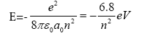
An ordinary negative electron and a positive electron, called a positron, situated a distance r apart in free space experience an attractive force called the Coluomb force, which has the value –e2/4πε0 r2, where e is their charge and ε0 is the dielectric constant of free space. A quantummechanical calculation shows that the electron and positron interact to form an atom called positronium which has bound-sate energies given by the Rydberg formula introduced by Niels Bohr in 1913 to explain the hydrogen atom
 (5)
(5)
Where a0 is the Bohr radius given by a0=4 πε0a0 h2/m0e2=0.0529 nm, m0 is the free-electron (and position) mass, and the quantum number n takes on the values n=1,2,3, ……∞. For the lowest energy or ground state, which has n=1, the energy is 6.8 eV, which is exactly half the ground-state energy of a hydrogen atom, since the effective mass of he bound electron-positron pair is half of that of the bound electronproton pair in the hydrogen atom. Figure shows the energy levels of positronium as a function of the quantum number n. This set of energy levels is often referred as a Rydberg series. The continuum at the top of the figure is the region of positive energies where the electron and hole are so far away from each other that the coulomb interaction no longer has an appreciable effect, and the energy is all of the kinetic type,  , or energy of motion, where v is the velocity and p=mv is the momentum.
We have carried out a new synthesis route to prepare powder form using combustion process. We also studied their photoluminescence exciting at different wavelengths.
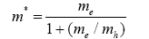
For a semiconductor the electron is in the conduction band, and the hole is in the valence band. The electron and hole both have effective masses me and mh, respectively, which are less than that (m0) of a free electron, so the effective mass m*=memh/(me+mh). When the electron effective mass is appreciably less than the hole effective mass, me«mh, the relationship between them is conveniently written in the form
 (6)
(6)
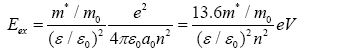
Which shows that for this case m* becomes comparable with the electron mass. For example, if me/mh=0.2, then m*=0.83 me. The relative dielectric constant ε/ε0 has the range of values 7.2<ε/ε0<17.7 for these materials, where ε0 is the dielectric constant of free space. Both of these factors have the effect of decreasing the exciton energy Eex from that of positronium, and as a result this energy is given by
 (7)
(7)
These same two factors also increase the effective Bohr radius of the electron orbit, and it becomes
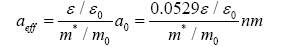
Using the GaAs electron effective mass and the heavy-hole effective mass valued from eqn. (5) gives m*/m0=0.226. Utilizing the dielectric constant value from, we obtain, E0=4.6 meV with the aid of eqns. (5) and (6) for NPs
aeff=21.06 nm (9)
Where E0 is the ground-state (n=1) energy. This demonstrates that an exciton extends over quite a few atoms of the lattice, and its radius in oxide materials is comparable with the dimensions of a typical nanostructure. An exciton has the properties of a particle; it is mobile and able to move around the lattice. It also exhibits characteristic optical spectra. The exciton that we a weekly bound electron-hole pair is called a Mott-Wannier exciton. A strongly or tightly bound exciton, called a Frenkel exciton, is similar to a long-lived excited state of an atom or a molecule. It is also mobile, and can move around the lattice by the transfer of the excitation or excited-state charge between adjacent atoms or molecules.
Electrical parameters-impedance analysis
Nyquist plot analysis is used to characterize bulk grain, grain boundary and electrode interface contribution from the successive semicircles of impedance exhibiting in the complex plane. This enables one to study the grain or bulk resistance (Rg) and grain boundary resistance (Rgb), which are useful in understanding the charge transfer phenomena. For the present MIS structure, only one semicircle in the intermediate frequency region is seen which is ascribed to the grain boundary contribution. This type of impedance variation can be represented as an equivalent circuit, which consists of a resistive element in parallel with a capacitor. This is the most common interpretation for polycrystalline oxide, having a contribution of rain boundary. The frequency at the semicircle maxima ωmax for each RC element is given by,
ωmax=2πfmax=(RC)-1=τ-1 (10)
Where, τ=RC is the relaxation time for the respective regions. Usually, the capacitance of the grain boundaries is larger than that of the bulk grain. Therefore, the relaxation time
τ=RC=ρεrεo (11)
is larger for the grain boundaries. The grain boundary resistance of the sample is extracted from the Nyquist plot, which is of the order of megaohm (28.19 MΩ). The capacitance value for the grain boundaries is calculated by noting the frequencies at the Debye peak maxima and is found to be in order of picofarad (14 pF). This result is in agreement with the reported values for the TiO2 thin film capacitors [5]. The relaxation time of the process is about 3.95 ×10⁻⁴ sec, which is due to the rotational fluctuations of molecular dipoles. If the frequency of the applied electric field corresponds to reorientation time (τ) of molecular dipoles, the imaginary part of impedance shows a characteristic pattern. In addition, the semicircular arc starts at the origin; hence, no series electrode resistance is included in the equivalent circuit representation.
The frequency and temperature dependence of Z’ (real part of the complex impedance) and Z” (imaginary part of complex impedance). It is observed that the magnitude of Z’ decreases with the increase in frequency and temperature. At high frequencies, Z’ values reach almost zero and this may be due to the release of space charges. The curve also display single relaxation process and indicate decrease in ac conductivity with frequency. The relaxation time (τ) is calculated from the frequency (fmax) at which Z”max is observed. The peak height is proportional to the grain boundary resistances according to the following equation in Z” vs. frequency plot,
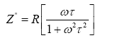 (12)
(12)
Moreover, in the Z” plot, the peak shifts towards higher frequency at the temperature increases. The magnitude of the imaginary component of the impedance at the peak frequency is also a strong decreasing function of temperature. An Arrhenius plot is drawn between 1000/T and ln (fmax) and the plot shows the thermally activated behavior and the corresponding activation energy is 0.28 eV which is in agreement with many of the dielectric ceramic capacitors [7]. The values of grain boundary resistance (Rgb) and grain boundary capacitance (Cgb) are evaluated from the Nyquist and Z”.
It is evident from figure that grain boundary resistance decreases and grain boundary capacitance increases with temperature. At lower temperature, the slope of the Nyquist plot is higher, yielding higher grain boundary resistance due to the insulating behavior of the material. With the rise in temperature, the slope of the plot decreases and makes the curves towards less resistive regions. The changes in ‘Rgb’ and the shift in Z” with temperature change the grain boundary capacitance accordingly.
The Bode plot explained at room temperature suggests the capacitive behavior of electrode as log Z varies linearly with log f. Slope of the curve is -0.974, which is very close to the theoretical value of -1 for a pure capacitor. Under this condition, ‘Z’ is related with frequency as,
log (Z)=-log(f) – log Cbl (13)
Where, ‘Cbl’ is the barrier layer capacitance. The value of Cbl obtained from is 0.93nF at room temperature. Also, it is obtained, the value of tan () at 40 Hz and 10 kHz are respectively 6.913 and 0.024. Dielectric loss factor tan (δ) at low frequencies are relatively large, which confirms the contribution of the d.c conductivity to the dielectric magnesium oxide.
Modulus analysis
The complex dielectric function ε* and its dependence on external electric field frequency and temperature originates from different processed like microscopic fluctuations of molecular dipoles, propagation of mobile charge carriers, polarization due to separation of charges at the interface etc. Contribution of polarization of charges at the interface to the dielectric loss can be orders of magnitude larger than the dielectric response due to molecular fluctuations. The microscopic and macroscopic processes have frequency and temperature dependence of the real and imaginary part of the complex dielectric function. The methods, to qualify the contributions to the dielectric function. The methods, to qualify the contributions to the dielectric spectra are discussed in this section.
Relaxation process are characterized by a peak in the imaginary partε” and a step like decrease of the real part ε’ of the complex dielectric function ε*=ε’-jε” with increasing frequency. In contrast, conduction phenomena show an increase of the imaginary part of the dielectric function with decreasing frequency. For pure ohmic conduction, the real part of ε* is independent of frequency and for non-ohmic conduction, the real part of ε* increases with decreasing frequency.
Further, the investigation of relaxation process that is related to the rotational fluctuation of molecular dipoles can be analyzed with the complex dielectric function ε*. If the frequency of the applied electric field equals the reorientation time ‘τ’ of the molecular dipoles, ε’ decreases with frequency and ε” exhibits a maximum. The frequency corresponds toε” maximum is the relaxation frequency of the fluctuating dipoles. The dipole strength Δε of a relaxation process can be determined from the loss peakε” or from the step in ε’.
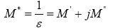
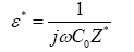
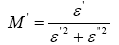
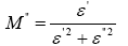
In order to allow accurate assessment of the impedance data, complex electric modulus formalism have been discussed for various dielectric materials [8]. In modulus formalism, the electric modulus M* is defined in terms of the reciprocal of the complex relative permittivity ε*.
 (14)
(14)
Where,
 (15)
(15)
 (16)
(16)
 (17)
(17)
‘C0’ is the vacuum capacitance of the sample holder.
The modulus data expressed in the complex modulus formalism enables to understand the phenomenon of conductivity relaxation in terms of variation of M’ and M” as a function of frequency as a function of frequency and temperature. The complex modulus plane analysis is based on the plot of imaginary part of M” against real part of M’ over a wide range of frequencies (40 Hz to 100 kHz reported in many studies) [9]. The plot is a single or a series of semicircular arcs. Each semicircular arc represents the parallel combination of resistance and capacitance of grain/grain boundary/electrode interface contribution in the conduction process. The semicircular arc in the low frequency region represents grain boundary/electrode interface contribution and an arc in the high frequency region represents the dominance of bulk grains. Magnesium oxide, the material considered in the present study exhibits a single semicircular arc in the low frequency region representing the dominance of grain boundary impedance. The impedance element representing the film/electrode interface is negligible because of lower value of contact resistance. Extracting the values of Rgb, the grain boundary resistance; Cgb, grain boundary capacitance and τ, the relaxation time are discussed in detail in the previous section. In this section, importance is given to the electric modulus response with frequency at different temperatures. The real and imaginary component of dielectric constant of the material is determined initially to find out the electric modulus M*.
Frequency dependence of real (ε’) and imaginary (ε”) parts of dielectric constant for the MgO thin film at different temperatures, both the pattern presents dispersion in the lower frequency region, while they merge above 1 kHz. It can be seen that at low frequency region, ε’ increases up to 50°C and then decreases, where as ε” gradually decreases with temperature. This may possibly be due to the electrical conductivity of the material that modifies the value of the capacitance as the temperature increases. Because of the polarization effect the real part of ε* increases with decreasing frequency [10].
The value of M’ is very low nearly zero at the low frequency region, a continuous rise with dispersion in high frequency region and have a tendency to saturate at a maximum asymptotic value designated M∝ for all temperatures. This observation may possibly be related to a lack of restoring force governing the mobility of charge carriers under the action of an induced electric field. This supports the long-range mobility of charge carriers. The step increase in the value of M’ may attribute to the short-range mobility of carriers. The variation of M” with frequency exhibits well-resolved peaks at characteristic frequency that depends on temperature. In addition, the peak positions have the tendency to move towards higher frequency side with the rise in temperature. The low frequency side of M” peak represents the range of frequencies in which the charge carriers can more over a long distance. Due to long-range mobility, the carriers can perform hopping from one site to the neighboring site. High frequency side indicates the range of frequencies in which the charge carriers are spatially confine to their potential well and therefore only localized motion within the well alone be possible. At the peak frequency region, the transition from longrange to short-range mobility is possible.
AC conductivity
Measurement of AC conductivity in insulating materials has been extensively used to understand the condition process in these materials. The generally accepted view is that the AC conductivity is dominated by localized states within the energy gap. Measurement of AC conductivity is therefore a powerful experimental method to obtain information about the localized states. Many workers [11] have carried out such measurements on a variety of materials.
In the present study, complex impedance spectroscopy (CIS) has been carried out for describing the electrical processes occurring in a system on applying an AC signal across the sample sandwiched between the electrodes. The output response of such an experimental measurement, when depicted in a complex plane plot, appears in the form of a succession of semicircles representing the contribution to the electrical properties due to the bulk material, grain boundary effect and interfacial polarization. CIS technique is therefore useful to separate the effects arising from each component in a polycrystalline sample very easily. Impedance measurements on a material provide data having both resistive (real part) and reactive (imaginary part) components. It can be displayed in a complex plane plot in terms of any of the formalism like complex impedance, complex admittance, complex permittivity, and complex modules. Moreover, the peak of the semicircular arc in the complex impedance spectrum provides the relaxation frequency of the material and their respective resistance and capacitances. The bulk conductivity (σdc) of the material is a thermally activated process obeying Arrhenius behavior, which can be estimated in terms of bulk resistance (Rb) evaluated from complex impedance spectrum. The bulk conductivity can be calculated in accordance with the relation,
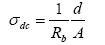 (18)
(18)
Where, ‘d’ is the thickness and ‘A’ is the area of the sample.
The AC conductivity of the material describing the frequency dependent behavior of the conduction process can be evaluated in accordance with the relation.
σAC=ωε’εo tan δ (19)
Where, tan δ is the dielectric loss, ε’ is the permittivity and ‘εo’ is the permittivity in vacuum.
For AC measurements, films were sandwiched between two electrodes. Top aluminium electrode is thermally evaporated on to the oxide film surface to a pre-defined area and the silicon substrate served as the bottom electrode. A programmable LCZ bridge was used to measure the impedance Z, the capacitance C and the phase ϕ directly. The total conductivity was calculated from the equation.
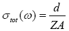 (20)
(20)
Where, ‘d’ is the thickness of the film and ‘A’ is the area of cross section of the sample. The dielectric constant (ε’) was calculated from the equation,
 (21)
(21)
Where, ‘εo’ is the permittivity of free space.
The dielectric lossε” was calculated from the equation,
ε”=ε’ tan δ (22)
Where, δ=90-ϕ and ‘ϕ’ is the phase angle.
The AC conductivity of oxide films were measured in the frequency and temperature ranges 40-100,000 Hz and 30-90°C respectively.
It is observed that σAC(ω) increases linearly with frequency. In addition, the plots show an onset at every temperature and the onset frequency shifts towards higher frequency side with the rise in temperature. The plot has two different regions with positive slopes and these regions arises due to the different conduction mechanisms σ1 and σ11. In both the regions, the conductivity variations are in accordance with the equation [12].
σAC(ω)=σtot(ω)-σDC=Aωs (23)
Where, ‘σDC’ is the DC part of the total conductivity σtot(ω), ‘s’ is the frequency exponent and ‘A’ is a constant.
It is evident that, the frequency variation of σDC(ω) involves a power exponent ‘s’ and assumed a value <1 in both the regions. In low frequency region s-parameter increases with temperature and in high frequency region it decreases. It shows large dispersion in the low frequency region as well as in high frequency region, they may coverage at high frequencies above 105 Hz. These variations indicate that the conduction process is a thermally activated process. The ac conductivity of the film increases with both frequency and temperature. To interpret the frequency and temperature dependence of AC conductivity, two models have been proposed by Austin, Mott [13] and Mason, et al. [14].
According to Austin and Mott, temperature dependent ac conductivity is due to thermally assisted quantum mechanical tunneling. In this QMT model, the AC conductivity dependence is expressed as,
σAC (ω)=A ωsTn (24)
Where, n=1 and the frequency exponent‘s’ is given by
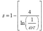 (25)
(25)
Where, τ is the characteristic relaxation time. The characteristic relaxation time increases with temperature and therefore ‘s’ increases with temperature or at least of temperature independent. In the present case, the s-parameter decreases with temperature in the high frequency region. Therefore, QMT model fails to explain the present conducting nature of the magnesium oxide films.
The concept of Pike and Elliot model is based on the concept of hopping between two change defect states over the barrier separating them. In this model, the temperature dependence of σAC(ω) obeys the equation,
n=-(1-s) ln (ωτ) (26)
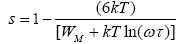 (27)
(27)
Where, ‘WM’ is the maximum barrier height.
The exponent‘s’ has values between 0 and 1 and decreases with temperature. In the present study, the temperature dependence of ‘s’ and their values in the range (0.47-068) are consistent with the correlated barrier hopping (CBH) model [15]. Further, the variation of ln(σAC) against 1000/T is linear over the entire temperature region and the conductivity obeys the Arrhenius relationship. The activation energies are obtained by least square fitting of the data. The activation energy is obtained by least square fitting of the data. The activation energy values are in the range 0.43-0.619 eV for the frequency region 0.1 kHz-100 kHz.
Conclusions
Oxide nanoparticles and thin film’s optical properties and its quantum confinement effect was discussed. The fabrication of MIS structures, and its Aluminium electrode was used as the metal top electrode. I-V measurements were carried out for a wide range of electric fields 20-20 × 104 V/cm. The conductivity mechanisms in the entire field range were identified from the current variations. Ionic ohmic region is observed in low fields, space charge effects in moderate fields and Poole Frenkel conduction in high fields. An increase of current with increase in the radiation doze was observed. The current transport mechanism in ion-implanted samples consists of trap assisted tunneling and thermionic emission. A decrease in zero bias potential barrier height with implantation fluence was also confirmed.
Complex impedance spectroscopic studies have been performed on the MIS structure to identify the dielectric behavior of the polycrystalline magnesium oxide thin films. Nyquist plot analysis was used to extract the impedance parameters. Bode equation analysis was used to study the capacitive behavior of electrodes. From the slope of the Bode plot, the purity of the capacitor and the barrier layer capacitance were determined. The effect of ion implantation on impedance parameters have been studied by both the impedance and electric modulus analysis. All the capacitors exhibit non-Debye type relaxation, showing distinct curves of Z”/Z”max and M”/M”max and the dipole polarization was only because of conduction of localized carriers.
References
- Brus L (1986) Electronic wave functions in semiconductor clusters: experiment and theory. The Journal of Physical Chemistry 90: 2555-2560.
- Efros AA, Leung TK (1999) Texture synthesis by non-parametric sampling. In: Computer Vision The Proceedings of the Seventh IEEE International Conference 2: 1033-1038.
- Tareke E, Rydberg P, Karlsson P, Eriksson S, Törnqvist M (2002) Analysis of acrylamide, a carcinogen formed in heated foodstuffs. Journal of agricultural and food chemistry 50: 4998-5006.
- Salières P, Carré B, Le Déroff L, Grasbon F, Paulus GG, et al. (2001) Feynman's path-integral approach for intense-laser-atom interactions. Science 292: 902-905.
- Green PF, Duddy IR, Gleadow AJW, Tingate PR, Laslett GM (1985) Fission-track annealing in apatite: track length measurements and the form of the Arrhenius plot. Nuclear Tracks and Radiation Measurements 10: 323-328.
- Hartman TE, Blair JC, Bauer R (1966) Electrical conduction through SiO films. Journal of Applied Physics 37: 2468-2474.
- Nyquist RA, Kagel RO (2012) Handbook of infrared and raman spectra of inorganic compounds and organic salts: infrared spectra of inorganic compounds. Academic Press 4.
- Perry MD, Stuart BC, Banks PS, Feit MD, Yanovsky V, et al. (1999) Ultrashort-pulse laser machining of dielectric materials. Journal of Applied Physics, 85: 6803-6810.
- Ahmad MM (2006) Ionic conduction and dielectric relaxation in polycrystalline Na2SO4. Solid state ionics 177: 21-28.
- Schönhals A (2003) Molecular dynamics in polymer model systems. In Broadband dielectric spectroscopy, pp: 225-293.
- Fukuda Y, Aoki K, Numata K, Nishimura A (1994) Current-voltage characteristics of electron-cyclotron-resonance sputter-deposited SrTiO3 thin films. Japanese Journal of Applied Physics 33: 5255.
- Jonscher AK (1977) The ‘universal’ dielectric response. Nature 267: 673-679.
- Austin IG, Mott NF (1969) Polarons in crystalline and non-crystalline materials. Advances in Physics 18: 41-102.
- Mason KO, Hassall BJM, Bromage GE, Buckley DAH, Naylor T, et al. (1995) Optical identification of EUV sources from the ROSAT Wide Field Camera all-sky survey. Monthly Notices of the Royal Astronomical Society 274: 1194-1218.
- Elliott SR (1987) Ac conduction in amorphous chalcogenide and pnictide semiconductors. Advances in Physics 36: 135-217.
Citation: Ayeshamariam A, Karunanithy M, Thirumamagal R, Nivetha S, Kavin MM, et al. (2017) A Review on Theoretical Studies of Optical and Electrical Parameters Values of Thin films. J Powder Metall Min 6: 177. DOI: 10.4172/2168-9806.1000177
Copyright: © 2017 Ayeshamariam A, et al. This is an open-access article distributed under the terms of the Creative Commons Attribution License, which permits unrestricted use, distribution, and reproduction in any medium, provided the original author and source are credited.
Select your language of interest to view the total content in your interested language
Share This Article
Recommended Journals
Open Access Journals
Article Tools
Article Usage
- Total views: 6386
- [From(publication date): 0-2017 - Dec 18, 2025]
- Breakdown by view type
- HTML page views: 5400
- PDF downloads: 986