Research Article Open Access
Studies on Different Doped Zn Concentrations of CdSe Thin Films
Rani S1, Shanthi J2, Kashif M3, Ayeshamariam A4* and Jayachandran M51Research Scholar, Bharathiar University, Coimbatore, Tamilnadu, India-641046
2Department of Physics, Avinashilingam University, Coimbatore, Tamilnadu, India-641043
3Department of Electrical and Electronic Engineering, Faculty of Engineering, Universiti Malayaia Sarawak 94300, Kota Samarahan Sarawak, Malaysia
4Department of Physics, Khadir Mohideen College, Adirampattinam, 614 701, India
5Department of Physics, Sree Sevugan Annamalai College, Devakottai, 630303, India
- *Corresponding Author:
- Ayeshamariam A
Department of Physics
Khadir Mohideen College
Adirampattinam, 614 701, India
Tel: 9443619470
Fax: +91-4565-227713
E-mail: aismma786@gmail.com
Received Date: June 21, 2016; Accepted Date: July 22, 2016; Published Date: July 30, 2016
Citation: Rani S, Shanthi J, Kashif M, Ayeshamariam A, Jayachandran M (2016) Studies on Different Doped Zn Concentrations of CdSe Thin Films. J Powder Metall Min 5:143. doi:10.4172/2168-9806.1000143
Copyright: © 2016 Rani S, et al. This is an open-access article distributed under the terms of the Creative Commons Attribution License, which permits unrestricted use, distribution, and reproduction in any medium, provided the original author and source are credited.
Visit for more related articles at Journal of Powder Metallurgy & Mining
Abstract
Different Zn concentration was doped with CdSe thin films by Electron Beam Evaporation method. Crystallite variation was studied for doping effect and it was found to be about 40 to 50 nm respectively. Optical band gap values are found to be modified by doping as well as annealing. Annealed films showed considerable influence in their optoelctronic and structural properties, which provided improvement in conversion efficiency of about 2.75% and 2.87% respectively.
Keywords
Electron beam evaporation; Doping effect; XRD of CdSe; PEC solar cells
Introduction
The formation of solid solutions in semiconductors is of great interest, since it yields new semiconducting materials such as ternary alloys. One of these, CdSe:Zn is particularly interesting for realization of electronic and applications for novel opto-electronic devices in the visible region of electromagnetic radiation [1]. The (ZnCd)Se system which enables a tuneable band gap region between 1.72 and 2.82 eV at normal temperature facilitates the development of several new electronic pulsations for light emitting diodes, photo detectors, blue green lasers, etc. [2]. As a wide band gap (2.42 eV at the room temperature) II-VI semiconductor, CdS is an excellent material that can be used for optoelectronic applications, such as nonlinear optics and light-emitting diodes. CdS is also a good active optical waveguide material and has electrically driven laser properties, which may find wide applications in telecommunications and data storage, highly integrated chemical/biological sensors, near-field optical lithography, and scanning probe microcopy. In addition, CdS is an efficient window material for solar cells such as those based on Cu2S, CdTe, CuInSe2, or CuInTe2. Thin films of these materials are usually synthesized by molecular beam epitaxy [3], electron beam evaporation [4] and chemical method [5].
Feng Ying et al. reported that few-layer graphene was prepared from highly oriented pyrolytic graphite by micromechanical cleavage and transferred to the silica on coated with silicon dioxide(SiO2/Si).The thickness of graphene on the SiO2/Si support was in vestigated by color and contrast variations, Chemical vapor deposition was also used to grow large area(~cm2) graphene [6].
Kang, et al. reported that, Colloidal photonic crystals were synthesized by a forced deposition method. A new micro-cell was developed through thermal deposition and micro-mechanical score, by replacing conventional photosensitive resin with Al thin film and polyether-sulfone membrane. Monodispersed colloidal polystyrene spheres with different sizes were used to deposit the colloidal photonic crystals in the micro-cell to confirm the validity of this method. SEM patterns and transmission spectra show that the crystals exhibit a facecentered cubic structure with low defect density, and the band gap agrees with the calculated result very well [7].
Feng Ying et al. reported that the enhancement of current on/off ratio in field effect transistor devices with bundled single-walled carbon nanotubes (CNTs) by incorporating a substrate etching step before the electrical cutting for metallic CNT elimination. The etching step prevents the damaging of the semiconducting CNTs while burning off the metallic ones by electrical current. By further incorporating a repeated gate voltage sweeping step, devices with low IoffIoff (less than 2 nA) and high Ion/IoffIon/Ioff, which is one to five orders of magnitude larger than before etching/cutting combination process, can be obtained [8]. These applications are very much helpful to explain doped thin films.
Experimental Section
Thin films of Zn doped CdSe were prepared by EBE technique using a HINDHI-VAC vacuum unit (model: 12A4D) fitted with electron beam power supply on glass substrates at room temperature (RT), followed by annealing at 200°C for 30 min. Well degreased microscopic glass plates have been employed as substrates in the present work. 500 mg of spectroscopically pure Cadmium selenide (99.99%) was mixed well with the selected dopants using a pestle and mortar. The mixture was pressed into pellets with a pressure of 500 kg/cm2, which was used as a source material for evaporation. The pellet was them taken in a graphite crucible and kept in water cooled copper hearth of electron gun. The pelletized CdSe targets, which were doped 10%, 20% and 30% Zn, were heated by means of an electron beam collimated from the dc heated tungsten filament cathode. The surface of the CdSe:Zn pellets were bombarded by 180° deflected electron beam with an accelerating voltage of 5 kV and a power density of~1.5 kW/cm2. The films were characterized by X-ray diffraction (XRD) studies using CuKα radiation from an X’pert Pro PAN-analytical XRD unit. Optical studies were made at room temperature using a Hitatchi-330 UV-Vis- NIR spectrophotometer. Atomic force microscopic (AFM) studies for morphological observations were conducted by Agilent technologies Model 5500. Photo anodes were prepared by depositing 0.5 cm × 0.5 cm area (0.25 cm2) of CdSe:Zn films on conducting coated glass substrates.
Results and Discussions
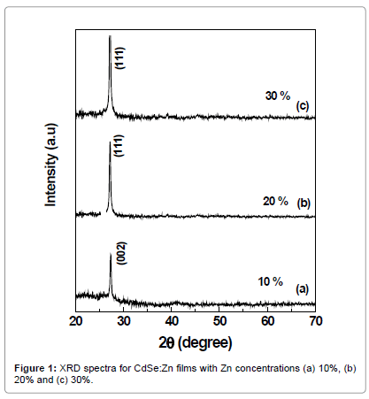
Zn doped CdSe films were deposited using electron beam evaporation (EBE) technique with optimized substrate temperature 100°C. Different concentrations of zinc (10%, 20% and 30%) were introduced into the CdSe matrix. Figure 1 shows XRD spectra of CdSe:Zn films with Zn concentrations 10%, 20% and 30% deposited at 100°C, respectively. All peaks are well defined and sharp peak indicated single phase of Cds:Zn samples. The peak observed at 2θ=25.61° corresponding to (002) orientation confirms the hexagonal structure of 10% Zn doped CdSe films while peaks at 26.48° and 27.32° corresponding to (111) orientation indicate cubic structure of 20% and 30% Zn doped CdSe films. The value of ‘x’ [9] describes single phase hexagonal (x < 0.5) or cubic structure (x > 0.5). Hence it is evident that the crystalline homogeneous and alloyed CdSe:Zn films can be grown in highly oriented single phase direction by vacuum evaporation technique. The lattice space ‘d’ values agree well with earlier reported XRD data [10] for the CdSe:Zn films deposited by electrochemical technique.
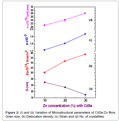
Microstructural parameters such as grain size, dislocation density, strain and lattice constant (a) values are given in Table 1. The lattice parameters of these films follow the Vegard’s law which means that the lattice parameters of Cd1-xZnxSe ternary alloys, with Zinc content ‘x’ linearly varies as lead binary alloy CdSe. It is noted that particle size decreases with increase in ‘Zn’ contents. Microstructural parameters plotted as a function of ‘Zn’ are shown in Figure 2. Husain et al. [11] reported cubic structure for the whole range of Zn content from x=0.2 to 0.8 for their sintered films. This result predicts that these ternary alloys all have hexagonal structure and CdSe-ZnSe composites forms highly mixed solutions by exact substitutions of Zn at the atomic locations of Cd [12-14].
| Zn concentrations | Grain size D (nm) | Dislocation density δ (x 1014) lines/m2 | Strain ε x 10-3 | No of crystallites n x 1015/unit area |
|---|---|---|---|---|
| 10% | 35 | 20.42 | 1.72 | 21.12 |
| 20% | 27 | 32.15 | 1.81 | 24.33 |
| 30% | 15 | 39.24 | 1.94 | 28.29 |
Table 1: Microstructural parameters of CdSe:Zn films deposited at 100°C (substrate temperature).
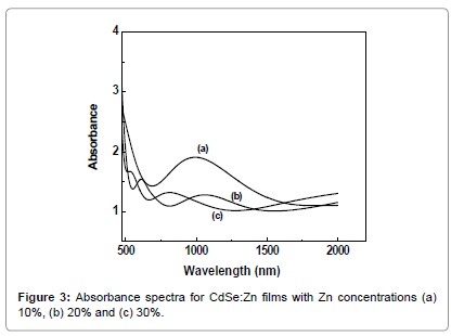
The doping with ‘Zn’ content strongly influences optical properties of the CdSe films. The optical absorbance and transmission spectra were recorded at room temperature in wavelength range of 300 to 2500 nm, as shown in Figures 3 and 4. The calculated optical band gap values (Eg) of CdSe:Zn thin films shown in Figure 5 with Zn concentrations 10%, 20% and 30% are 1.90, 2.26 and 2.42 eV, respectively. It is clearly seen that value of Eg is increased with increase in the Zn concentration. In highly doped semiconductors several effects contribute to change of the energy gap value corresponding to the parent material. The optical transition energy increases which shrink the band gap due to formation of doping band tails. The increase in optical band value of CdSe:Zn films might be due to the presence of high energy gap material (ZnSe) than that of undoped CdSe. The variation of Eg shows a sublinear behaviour, a lowering phenomenon in the alloy films of CdSe:Zn [15]. The as-prepared films exhibited direct band-gap transition and the absorption edge shows a blue-shift with increasing ‘Zn’ content due to the increase in band gap value. The continuous variation of Eg with Zn concentrations confirms the solid solution formation between CdSe and ZnSe so that their optical and electronic properties can be tailored according to the need for device developments.
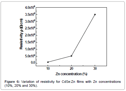
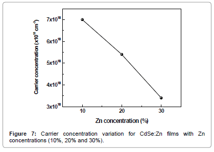
The electrical resistivity and the interface behaviour of semiconductor thin films with solid solutions are vital in photoelectrochemical solar cell applications. At room temperature the observed resistivity of CdSe:Zn films with 10%, 20% and 30% Zn content was 8.2 × 10⁴, 5.3 × 10⁵ and 3.5 × 10⁶ ohm cm respectively. The increase in resistivity is attributed to fact that band gap increases with introduction of more zinc into the lattice of CdSe. The higher resistivity CdSe:Zn films finds an application as a buffer layer for solid state solar cells. It is attributed to excess of Cd in the compostion over Se, which well separates conduction and valence bands in the crystal lattice [16]. The calculated carrier concentration values are 7.0 × 10¹⁸, 5.4 × 10¹⁸ and 3.4 × 1018 cm-3 for CdSe:Zn films with zinc content 10%, 20% and 30% respectively are shown in Figures 6-8.
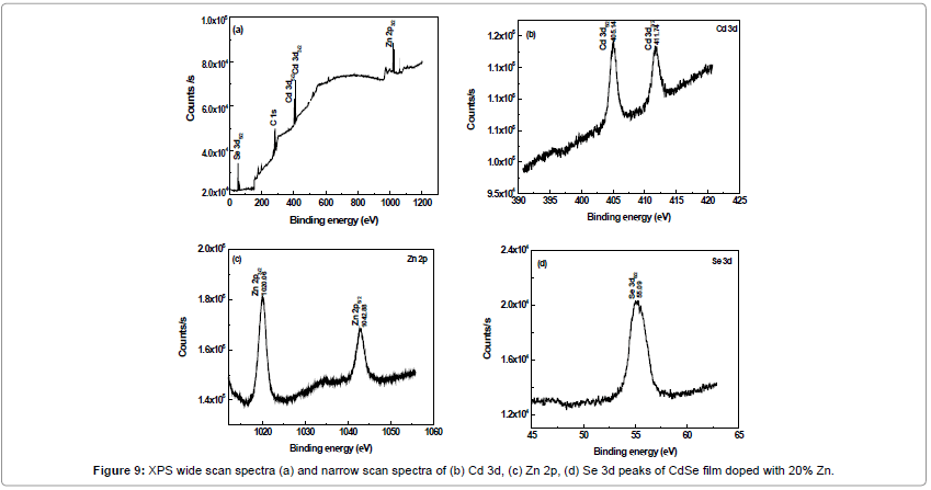
Figure 9a shows XPS spectra of CdSe:Zn film with zinc content 20% deposited at 100°C. It shows the presence of Cd ‘3d, Zn ‘2p and Se ‘3d peaks confirming the formation of Zn doped CdSe film. Figure 9b-9d shows the narrow spectra of Cd 3d, Zn 2p and Se 3d present in the film. The spectral shift along with the abscissa due to the sample charging is eliminated by moving the measured C 1s peak to the binding energy value of 284.8 eV [17]. In Figure 9b, binding energies of Cd 3d5/2 and 3d3/2 are observed at 405.14 and 411.74 eV which confirms the presence of Cd while Se 3d peak is seen at 55.09 eV which may be assigned to the presence of Se. Zn 2p3/2 and 2p5/2 peak is located at 1020.06 eV and 1042.88 eV respectively which confirms that Zn has been successfully doped in the prepared CdSe film.
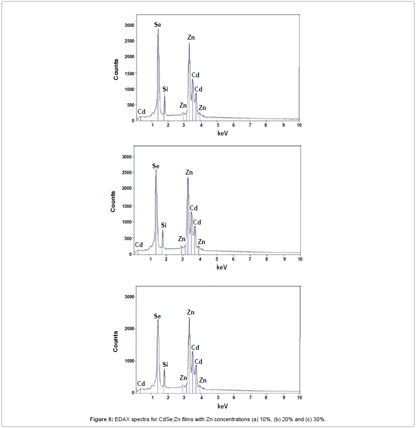
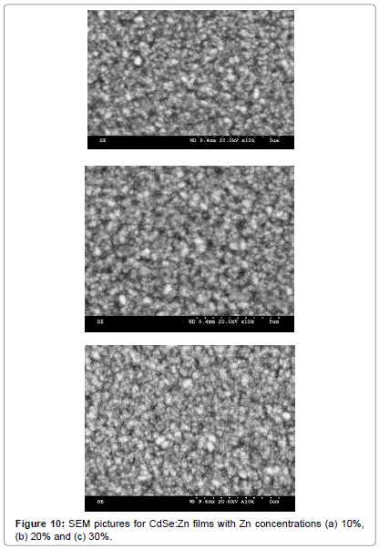
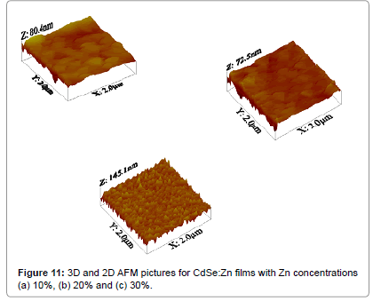
Figure 10a-10c shows SEM results of small and fine grains smeared all over the surface of Zn doped with CdSe films which is characteristic features of zinc rich surfaces [18]. Figure 11a-11c shows two (2D) and three dimensional (3D) AFM images of AFM with 10%, 20% and 30% Zn doped with CdSe films respectively. The average surface roughness (Ra) for these films show very low values 0.18, 0.24 and 0.30 nm respectively that corresponds to uniform surface of CdSe:Zn film prepared by the EB evaporation technique which is confirmed by the line profile curves given under each 2D AFM pictures. Figure 9a-9c shows the elemental analysis of CdSe:Zn films with zinc content 10%, 20% and 30% respectively. It is found that ratios of Cd and Zn elements are in fewer amounts than the percentage present in the initial material but selenium content is always present in stoichiometric percentage.
It is well observed that zinc atoms replace cadmium atoms in the crystal lattice and size of the grain is decreased with increasing the Zn contents. It might be caused by the addition of CdSe to ZnSe that reduce the dimension of the lattice leading to the formation of linear grains with reduced grain size. It shows the compactness, pinhole free and well adherent nature of these films on glass substrates which are very useful for PEC devices. This is attributed to the fact that the CdSe is consequently sublimation takes place first, and then reaches the substrate over which ZnSe gets deposited when they are grown by EB evaporation technique [19,20].
Photoluminescence properties depend on the lateral size of interface defects, as compared to the exciton diameter. The case of a pseudo-smooth interface applies when the exciton size is larger. This results in a relatively narrow single PL line, because the exciton properties are averaged over a number of defects. Ternary alloy semiconductor films has provided possibility of making their band gap (Eg) adjustable in the visible wavelength range and it is therefore useful for optoelectronic applications and devices as laser diodes and light emitting devices operating in the spectral region from red to green [21]. For such applications, a good PL efficiency is required for the CdSe:Zn system to assess them for optoelectronic applications.
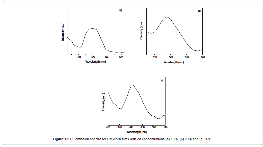
Figure 12a-12c shows the PL emission spectra recorded at room temperature. PL peak are observed at 622, 519 and 482 nm while Eg values are 1.99, 2.36 and 2.60 eV corresponding to the films CdSe:Zn films with zinc contents 10%, 20% and 30% respectively. The peaks shifts towards higher energy values were observed with increasing zinc concentration which is attributed to the increase in band-gap caused by ZnSe composition. Each PL spectrum is characterized by its near band edge (NBE) recombination as suggested for the CdSxSe1-x films prepared by pulsed laser deposition technique [22]. PL peak attained at 5K for Cd0.23Zn0.77Se single quantum well (QW) at about 2.77 eV with 0.4 ML (monolayer) and at 2.73 eV with 1.15 ML [23]. Photoluminescence results confirm solid solution CdSe:Zn films deposited by EB evaporation technique can efficiently be used for PEC solar cells and light emitting diode studies
Conclusions
Using EB evaporation technique CdSe:Zn thin films were prepared on glass substrates at 100°C with Zn concentration of 10%, 20% and 30%, respectively. Nanocrystalline nature of as-prepared films was characterized using XRD analysis. Optical studies were conducted to record absorbance and transmittance spectra of CdSe:Zn films. The absorbance curves, band gap values calculated from (αhν)2 vs (hν) curves showed direct band gap nature of all the films with band gap values varied from 1.90 eV to 2.42 eV. This confirmed solid solution formation between CdSe and ZnSe compounds and the lattice modification is effected by zinc incorporation. Elemental analysis was carried out by EDAX and XPS. The surface morphology explored by SEM analysis showed highly fine granular grain formation distributed uniformly over the entire surface. The influence of the variation of zinc content can be explicitly seen by the changing surface grain patterns from AFM studies. Photoluminescence (PL) technique is used to assess for material application to certify that CdSe:Zn films are good for the fabrication of PEC cell.
References
- Gupta P, Maiti B, Chaudhuri S, Pal AK (1995) Photoconductivity and Thermoelectric Power of ZnxCd1-xSe Films.Jpn J ApplPhys 34: 4658.
- Samarth N, Luo H, Furdyna JK, Qadri SB, Lee YR (1990) Surf Sci 228:226.
- Feng RZ, Guo SP (1994) The structure and strain relief in epitaxially grown CdSe on ZnSe by atomic layer epitaxy. J Mater SciLett 15: 1824.
- Islam R, Rao DR (1994) Electrical properties of polycrystalline Zn1−x Cd X Se thin films grown by electron beam evaporation. J Mat SciLett 13: 1637.
- Pandey RK, Rooz AJN, Gore RB (1988) Chemically formed Cd1-xZnxSe photo-anodes: II. Preparation, electrical, photoelectrochemical and solar cell studies. SemicondSci Tech 3: 733.
- Feng Y, Huang SH, Kang K, Duan XX (2011)Preparation and characterization of graphene and few-layer grapheme. New carbon materials, 26: 26-30.
- Kang K, Huang SH, Feng Y, Dong LQ, Zhu LAY (2008) Fabrication of Colloidal Photonic Crystals by a Micro-cell Based on Al Thin Film.66: 1615-1619.
- Feng Y, Lee K, Farhat H, Kong J (2009) Current on/off ratio enhancement of field effect transistors with bundled carbon nanotubes. Journal of Applied Physics 106: 104505.
- Gupta P, Marity B, Marity AB, Chaudhuri S, Pal AK (1995). Thin Solid Films 260: 75.
- Chandramohan R, Maha lingam T, Chu JP,Sebastian PJ (2004) Preparation and characterization of semiconducting Zn1− xCdxSe thin films. Sol Ener Mater Sol Cells 81: 371.
- Husain M, Sing BP, Kumar S, Sharma TP, Sebastian PJ (2003) Optical, electrical and structural investigations on Cd 1− x Zn x Se sintered films for photovoltaic applications. SolEner Mater Sol Cells 76: 399-415.
- Al Bassam A, Brinkumar AW, Russel GJ, Woods J (1988) J Cryst Growth 86: 667.
- Nasilov AS, Korostelin YV, Shapkin V, Suslina LG, Fedrov DL, et al, (1989) Solid State Comm 71: 867.
- Bis RF, Dixon JR (1969) J Appl Physics 40: 1918.
- Hill R, Richardson D (1973) The variation of energy gap with composition in ZnS-Te alloys.J Phys C 6: L 115.
- Sze SM (1981) Physics of Semiconductor Devices, 2nd ed., Wiley, New York, NY.
- Chen KT, Shi DT,Chen H, Granderson B, George MA, et al. (1997) Study of oxidized cadmium zinc telluride surfaces. J VacSciTechnolA 15: 850.
- Eser E, Hall RB (1981)Grain Structure of CdS and (CdZn)S Films. Thin Solid Films 86: 31.
- Islam R, Banerjee HD, Rao DR (1995) Structural and optical-properties of cdsexte1-x thin-films grown by electron-beam evaporation. Thin Solid Films 266: 215.
- Burmeister RA, Stevenson DA (1967) Phase Equilibria in the Cd‐Se System. J ElectrochemSoc 114: 394-398.
- Perma G, Pagliana S, Capozzi V, Ambrica M, Pallana M (2000) Solid State Comm. 114: 161.
- Perma G, Pagliara S, Capoyzi V, Ambrico M, Ligonzo T (1999) Thin Solid Films 349: 220.
- Toropov AA, Shubina TV, Socokin SV, KyuttRN,Ivanov SV,et al. (2000) Appl SurfSci 166: 278.
Relevant Topics
- Additive Manufacturing
- Coal Mining
- Colloid Chemistry
- Composite Materials Fabrication
- Compressive Strength
- Extractive Metallurgy
- Fracture Toughness
- Geological Materials
- Hydrometallurgy
- Industrial Engineering
- Materials Chemistry
- Materials Processing and Manufacturing
- Metal Casting Technology
- Metallic Materials
- Metallurgical Engineering
- Metallurgy
- Mineral Processing
- Nanomaterial
- Resource Extraction
- Rock Mechanics
- Surface Mining
Recommended Journals
Article Tools
Article Usage
- Total views: 11883
- [From(publication date):
December-2016 - Aug 30, 2025] - Breakdown by view type
- HTML page views : 10865
- PDF downloads : 1018

