Dersleri yüzünden oldukça stresli bir ruh haline sikiş hikayeleri bürünüp özel matematik dersinden önce rahatlayabilmek için amatör pornolar kendisini yatak odasına kapatan genç adam telefonundan porno resimleri açtığı porno filmini keyifle seyir ederek yatağını mobil porno okşar ruh dinlendirici olduğunu iddia ettikleri özel sex resim bir masaj salonunda çalışan genç masör hem sağlık hem de huzur sikiş için gelip masaj yaptıracak olan kadını gördüğünde porn nutku tutulur tüm gün boyu seksi lezbiyenleri sikiş dikizleyerek onları en savunmasız anlarında fotoğraflayan azılı erkek lavaboya geçerek fotoğraflara bakıp koca yarağını keyifle okşamaya başlar

GET THE APP

Modelling Of An Ionic Phototransistor Effect For The Characterization Of A Semiconductor Structure | 18731
ISSN: 2155-9872

Journal of Analytical & Bioanalytical Techniques
Open Access

Our Group organises 3000+ Global Conferenceseries Events every year across USA, Europe & Asia with support from 1000 more scientific Societies and Publishes 700+ Open Access Journals which contains over 50000 eminent personalities, reputed scientists as editorial board members.

Open Access Journals gaining more Readers and Citations
700 Journals and 15,000,000 Readers Each Journal is getting 25,000+ Readers
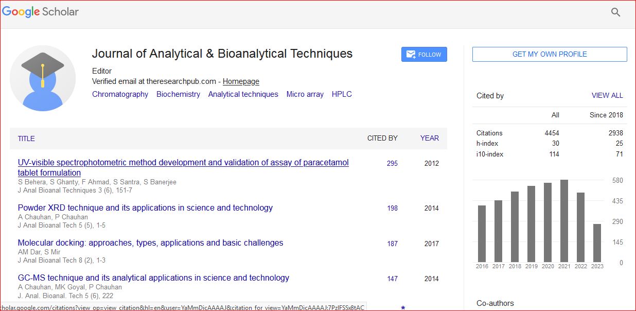
This Readership is 10 times more when compared to other Subscription Journals (Source: Google Analytics)

Modelling of an ionic phototransistor effect for the characterization of a semiconductor structure

5th International Conference and Exhibition on Analytical & Bioanalytical Techniques

A G Rokakh, A A Serdobintsev, V A Aleksandrov, M I Shishkin, S B Venig and I A Kornev

Accepted Abstracts: J Anal Bioanal Tech

DOI: 10.4172/2155-9872.S1.019

Abstract
Earlier it has been shown by us that target illumination can increase an exit of positive ions (a so-called anomaluos secondary-ionic photoeffect). This report concerns semiconductor-dielectric structure Su-GaAs-AlGaAs-SiO-Cu. The Сu film electrode on the side GaAs was carried out continuous, and on the side SiO - in the form of interdigital combs. Attaching contacts to each of combs and to the continuous electrode, we receive the three-electrode structure which characteristics depend on a power supply circuit of constant voltage. This structure consists of two circuits equal in rights each of them includes the general electrode and one of combs. At electric measurements influence of one chain on another that is characteristic for the transistor was revealed. As the initial semiconductor heterostructure possessed photoconductivity mutual influence of chains was supplemented with light control. Thus, we deal with phototransistor structure. At a premise of such structure in ultrahigh vacuum of a mass spectrometer possibility of management of an exit of secondary ions by means of illumination of different spectral structure, and also change of size and polarity of the enclosed voltage is reached. Such a semiconductor-dielectric structure allows to operate, on the one hand, an output of secondary ions (technological control), and with another - supposes use for a characterization of the structure. Thus it is possible to define a doping profile, depth of the electron-hole junction, photosensitivity etc. The told above allows to consider that we deal with the device of optoionics - new area of a science and the technology which is born at research of influence of light on an output of secondary ions from photosensitive target, received the name of a secondary-ionic photoeffect.
Biography
A G Rokakh graduated from Physical Department of the Saratov N.G. Chernyshevsky State University in 1957 and continued his work as a scientific researcher and a teacher. He is a professor of the nano- and biomedical technology department of the mentioned university. He has above 350 publications in various fields, mainly in semiconductor physics. He was a member of the desk board of the international journal Physics Express and a nominator of Prof. A. G. Rokakh Award for the best paper in semiconductor physics of the same journal; the full member of the American Nano Society.
Top