Analytical Vth, DIBL and Swing with and without Effective Conducting Path Effect (ECPE) for the Submicronic SDG FD SOI MOSFET
Received: 02-Nov-2015 / Accepted Date: 10-Dec-2015 / Published Date: 16-Dec-2015
Abstract
We are presenting a convergence study of the evanescent model and the polynomial model with and without the Effective Conduction Path Effect (ECPE). These analytic models of the electric potential in the channel are used to analyze the short channel effect for the submicronic Symmetric DG FD SOI MOSFET. In this paper, we figure out the 2D Poisson equation and we analytically write using the evanescent model, the surface potential, the threshold voltage, the DIBL and the sub-threshold swing. The natural scale length for the polynomial model λp and its corrected form λpc including the ECPE are mentioned. The results, of the analysis of the short-channel effects (SCEs), show a good agreement of the evanescent model and the polynomial model including the ECPE with measures done by simulation tools.
Keywords: Evanescent and polynomial models; Effective conduction path effect; Surface potential; Threshold voltage; DIBL; Sub-threshold swing; Symmetric double gate fully depleted SOI MOSFET
18086Introduction
The electronic industrial world is in continuous search for an amelioration of the speed and the consumed power of the MOSFET device. But, with the miniaturization of the shape, governed by the ITRS roadmap [1], this component has shown its defects due to the parasitic effects. Among these undesirable effects, the so called short channel effects (SCEs), which minimize the MOSFET performances [2] and perturb the IC function.
The microelectronic industrials have sought to avoid these defects. The MOSFET structure on silicon with multiple gates [3-6] has proved successful in increasing the duration of the miniaturization and improving the compound performances taking into consideration the preservation of the planar silicon technology.
Despite its complex technological realization, the Symmetric DG FD SOI MOSFET remains one of the most interesting and encouraging compound to realize the Ultra-Deep Sub-Micronic (UDSM) structure and throughout augment density of integration.
Many models [7-13] have been developed to examine the performance of components. In this paper, we will put the evanescent model and the polynomial model with and without the ECPE into consideration to find out their convergence points for the study of the SDG FD SOI MOSFET. We solve the 2D poisson equation and we, analytically, analyze the SCEs via the dispersion study of the surface potential and the threshold voltage along the channel as well as the DIBL effect and the sub-threshold swing. The natural scale length for the polynomial model λp and its corrected form λpc including the ECPE are mentioned. The analysis of the SCEs allows us to locate the convergence points of the utilized models. We confirm these convergence situations by simulator data and/or some measures.
Evanescent Model
Surface potential and threshold voltage
Figure 1 illustrates the cross section of the symmetrical DG SOI MOSFET device under fully depleted conditions and the inversion charge is neglected in regard to that of the of the depletion. We define by L, distance between source and drain, the channel length. tox and tsi represent respectively the thickness of the frontal oxide and the silicon body thickness. Na is the silicon doping in the channel and Nd is the doping concentration of the source and drain regions. εsi and εox represent respectively the dielectric permittivity of the silicon film and the silicon dioxide.

Figure 1: Schematic cross section of a symmetric DG FD SOI MOSFET device.
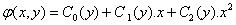
The evanescent model supposes that the electrostatic potential in the silicon film, overlapped between both grids, is represented, according to the superposition principle, by φ(x,y) = φ1(x)+ φ2(x,y). φ 1(x) is the solution of Poisson equation for a long channel and φ2(x,y) is the solution of the Laplace equation and contain the short channel effect [14].
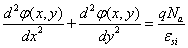 (1)
(1)
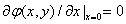
The necessary boundary conditions of φ1 and φ2 to define φ(x) are as follow:
For φ1:
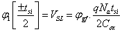

Where φgf = Vgf-Vfb, VSL represents the surface potential for a long channel at  ; Vfb is the flat band voltage at the interface grid oxide – poly-silicon substrate.
Cox =[εox/tox ] is the frontal oxide capacitance and Csi = [εsi/tsi ] is the silicon body capacitance.
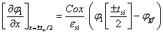
For φ2:
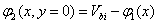
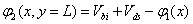

Where  denotes the built-in voltage between the source/drain end.
The frontal surface potential is defined as:

and written as follow:
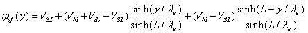 (2)
(2)
Where λe represents the characteristic length for the evanescent model and verify the follow equality:
 (3)
(3)
The threshold voltage is defined as a grid voltage (Vgf=Vth) for φsf=2∅B at y=y0 where 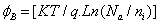 is the Fermi potential in the channel and y0 is the minimum surface potential abscise. This leads to write Vth as the form:
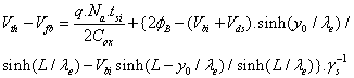 (4)
(4)
Where γs denotes the short channel effects [15] and written as:

The gradient of threshold voltage is defined as ΔVth =Vth0-Vth where Vth0 denotes the threshold voltage for a long channel SDG FD SOI MOSFET and written as:
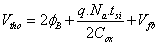 (5)
(5)
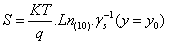
DIBL parameter
For the SDG FD SOI MOSFET with short channel, the surface potential minimum increase with the drain bias. Thus, the short channel effect is attributed to the penetration of the electric field line, of the drain-channel junction, in the channel resulting in the potential barrier lowering (DIBL effect). This leads to the decreasing of the threshold voltage.
The ℜ parameter defined by  evaluates the DIBL effect and written as:
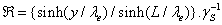 (6)
(6)
Sub-threshold swing
The sub-threshold slope, appealed swing, is defined as the grid voltage that modifies the drain current under a threshold of a decade and written as
 (7)
(7)
Where y0 is the minimum surface potential abscise.
Polynomial Model
Without the ECPE
Taking into account the polynomial model which considers the conduction current is at the surface of the silicon body and supposes parabolically the electrostatic potential profile in the vertical direction [6,10].
 (8)
(8)
Using the classical boundary conditions:

and writing the Poisson equation as 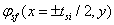 , we deduce the polynomial characteristic length
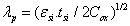 (9)
(9)
Including the ECPE
The notion of the ECPE supposes that the gravity centre of the conduction current is at x=deff. The presentation of the electrostatic potential φ( x, y) at x=deff allows us to bring about a correction to polynomial characteristic length λp.
The new corrected characteristic length corresponding to the polynomial model including ECPE is:
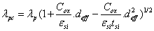 (10)
(10)
The key factor deff, which illustrates the variation of scaling nature length λpc with substrate doping density, is so-called depth of the effective conducting path and it presents the location where the punch through current mainly occurs at subthreshold conduction with ECPE conducting mode [10].
The evanescent model and the polynomial model with and without the ECPE are utilized to analysis the short channel effect with the intention of searching the situations of their convergence.
Results And Discussion
To verify the analytical models of the convergence of SCE’s, the graphs illustrating le surface potential, the threshold voltage, DIBL and swing were plotted, compared and verified by measurement data. The same work for the conventional MOSFET prove that the convergence situation for the evanescent model and the polynomial model including ECPE is at deff=0.5tsi [16] and at deff=0.35tsi [17] for the single-gate SOI MOSFET device.
For the three models, figure 2 shows the evolution of the characteristic length λi (i=e, p or/and pc) as a function of ratio (tox/ tsi) for Na=4.1017cm-3, Vds=0.5V and for a large range of tsi (tsi=1,5 and 10nm). We notice an adequate convergence, at deff=0.25tsi, between the evanescent model and the polynomial model including the ECPE. We also see that this convergence situation coincide with the data of equation 27 cited by Chen [13].

Figure 2: Characteristic length λi =5 versus ratio (tox/tsi).
Figure 3 presents the evolution of the surface potential minimum and its position along the channel for the submicronic SDG FD SOI MOSFET device and for Vds=0.5 and 2.5V. The results, and on a large scale of drain bias, show a good agreement between the evanescent model and the polynomial model including the ECPE at deff=0.25tsi.

Figure 3: Minimum channel surface potential and its location y0 as a function of position along the channel for different values of drain bias.
Figure 4 illustrates the evolution of the threshold voltage gradient in regard to the normalized position to L along the channel for L=150nm, Vds=1.5V, tox=1.5nm and for tsi=5, 10 and 25nm. These results prove a perfect agreement, at deff=0.25tsi, between the evanescent model and the polynomial model including the ECPE with Jaju’s measurements [11].

Figure 4: Variation of threshold voltage gradient versus normalized position along the channel y/L.
As the drain voltage increases, the channel barrier and the threshold voltage are reduced. This is called Drain Induced.
Barrier lowering. Figure 5 shows the evolution of the DIBL parameter as function of normalized position along the channel for the ultra-thin SDG FD SOI MOSFET with L=150nm, Vds=1.5V, tox=1.5nm and for tsi=5 and 10nm. Measures data [11] agree closely with the predictions of the evanescent model and the polynomial model including the ECPE at deff=0.25tsi.

Figure 5: DIBL parameter versus normalized position along the channel y/L.
Figure 6 presents the sub-threshold swing parameter, in weak inversion, as a function of normalized position a channel length for tox=1.5nm, tsi=10nm, Na=1.1017cm-3 and Vds=1V [11] and for tox=1.5nm, tsi=20nm, Na=1.1016cm-3 and Vds=1V. We notice an adequate convergence, at deff=0.25tsi, between the evanescent model and the polynomial model including the ECPE with Jaju’s measurements [11] as well as those of MEDICI’s [14].

Figure 6: Variation of the Sub-threshold Swing with normalized position along the channel y/L.
Conclusion
The study of the short channel effects through the surface potential, the threshold voltage, the DIBL and the sub-threshold swing has proved the convergence situation of the evanescent model and the polynomial model including the ECPE. The convergence situation for the ultrathin SDG FD SOI MOSFET’s device is at deff=0.25tsi.
References
- International Technology Roadmap for Semicondu ctors: ITRS 2008 Edition: 2008 Update
- Diagne B, Prégaldiny F, Lallement C, Sallese JM, Krummenacher F (2008) Explicit compact model for symmetric double-gate MOSFETs including solutions for small-geometry effects. Solid-State Electronics 52: 99-106.
- Colinge JP (2004) Multiple gate SOI MOSFETs. Solid-State Electronics 48: 897-905.
- Oh SH, Monroe D, Hergenrother JM (2000) Analytic description of channel effects in fully depleted double gate and cylindrical, surrounding gate MOSFET's. IEEE electron device letters 21: 445-447.
- Cristoloveanu S (2008) How many gates do we need in a transistor: one, two, three or four?.Romanian Journal of Information Science and Technology 11: 17-28.
- Aouaj A (2010) Analytical study of short channel effects in fully depleted double gate and cylindrical gate MOSFETs. J. of Active and Passive Electronics Devices 5: 121-127.
- Amara A, Rozeau O (2009) Planar double-gate transistor. Technology to circuit Springer Science
- El-hamid HA, Roig J, Iniguez B (2007) Analytical predictive modeling for the study of the scalability limits of multiple gate MOSFETs. Solid-State Electronics 51: 414-422.
- Aouaj A, Bouziane A, NouaçryA (2005) Analytical 2D modeling for potential distribution and threshold voltage of the short channel fully depleted cylindrical/surrounding gate MOSFET. Int. J. of Electronics 92: 437-443.
- Chiang TK (2005) A new scaling theory for fully depleted SOI double gate MOSFET's: including effective conducting path effect (ECPE). Solid-State Electronics 49: 317-322
- Jaju V (2004) Silicon-on-insulator technology EE 530. Advances in MOSFETs Spring
- Sallese JM, Krummenacher F, Prégaldiny F, Lallement C, Roy A, et al. (2005) A design oriented charge bead current model for symmetric DG MOSFET and its correlation with the EKV formalism. Solid-State Electronics 49: 485-489.
- Chen Q, Harrell EM, Mendl J (2003) A physical short-channel threshold voltage model for undoped symmetric double-gate MOSFETs. IEEE Transactions on electron devices 50: 1631-1637.
- Chen Q, Agrawal B, Moendl J (2002) A comprehensive analytical sub threshold swing (S) for double-gate MOSFETs. IEEE Transactions on electron devices 49: 1086-1090.
- Godoy A, Lopez-Villanueva JA, Jimenez-Tejada JA, PalmaA ,Gamiz F (2001) A simple sub threshold swing model for short channel MOSFET's. Solid-State Electronics 45: 391-397.
- Bouziane A, Aouaj A, Nouaçry A (2009) Comparison between the evanescent model, the polynomial model and the polynomial model including effective conduction path effect: applied to the submicronic MOSFET. IEEE International Conf. on Multimedia Computing and System Ouarzazate-Morocco 313-316.
- Bouziane A, Aouaj A, Nouaçry (2010) Investigation on the convergence of the evanescent model and the polynomial model including effective conduction path effect (ECPE): applied to thesubmicronic SG FD SOI MOSFET. MJ Condensed Matter 12: 238-243.
Citation: Nouacry A, Bouziane A, Aouaj A, Touhami A (2015) Analytical Vth, DIBL and Swing with and without Effective Conducting Path Effect (ECPE) for the Submicronic SDG FD SOI MOSFET. Innov Ener Res 4: 127.
Copyright: ©2015 Nouacry A, et al. This is an open-access article distributed under the terms of the Creative Commons Attribution License, which permits unrestricted use, distribution, and reproduction in any medium, provided the original author and source are credited.
Select your language of interest to view the total content in your interested language
Share This Article
Recommended Journals
Open Access Journals
Article Usage
- Total views: 12898
- [From(publication date): 12-2015 - Aug 29, 2025]
- Breakdown by view type
- HTML page views: 11910
- PDF downloads: 988