 Spanish
  Chinese
  Russian
  German
  French
  Japanese
  Portuguese
  Hindi
Hindi Our Group organises 3000+ Global Conferenceseries Events every year across USA, Europe & Asia with support from 1000 more scientific Societies and Publishes 700+ Open Access Journals which contains over 50000 eminent personalities, reputed scientists as editorial board members.
Open Access Journals gaining more Readers and Citations
700 Journals and 15,000,000 Readers Each Journal is getting 25,000+ Readers
Google Scholar citation report
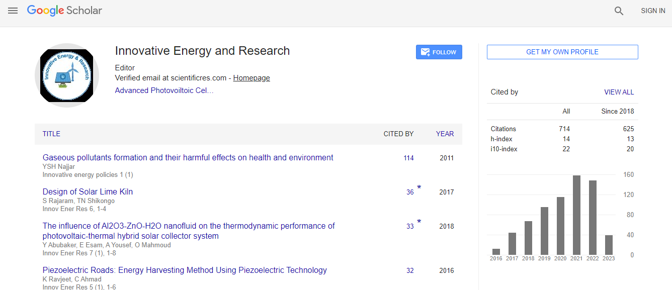
Citations : 712
Innovative Energy & Research received 712 citations as per Google Scholar report
Innovative Energy & Research peer review process verified at publons

Indexed In
- Google Scholar
- Open J Gate
- Genamics JournalSeek
- RefSeek
- Hamdard University
- EBSCO A-Z
- Publons
- Euro Pub
- ICMJE
Useful Links
Recommended Journals
Related Subjects
Share This Page
Reactive plasma processes for formation of high-mobility IGZO thin film transistors
21st International Conference on Advanced Energy Materials and Research
Yuichi Setsuhara
Osaka University, Japan
Keynote: Innov Ener Res
Abstract
Reactive plasma process systems have been developed via installation of inductively-coupled plasmas (ICP) sustained with low-inductance antenna (LIA) for low-temperature fabrication of flexible electronics, which require large area and low damage processes with reactivity control capabilities at low substrate temperature. Major advantage of the reactive processing system is that the reactivity during film-deposition processes can be enhanced and controlled via low-damage and high-density plasma production for low-temperature processing of devices. The reactive plasma processes have been applied to sputtering deposition of transparent amorphous oxide semiconductor a-InGaZnOx (a-IGZO), which has attracted great attentions as key material for next-generation flexible electronics. So far post annealing at elevated temperature (as high as 400°C) was required. Thus the conventional process for fabrication of the IGZO TFTs has been carried out on glass substrates. With the advanced reactivity controlled plasma processes in this study, a-IGZO thin-film transistors (TFTs) with mobility as high as or higher than 40 cm2/Vs was successfully formed at substrate temperature less than 200°C. In this presentation, the reactive plasma processes are presented for low-temperature formation of IGZO TFTs.Recent Publications
1. K Takenaka, M Endo, G Uchida and Y Setsuhara (2018) Fabrication of high-performance InGaZnOx thin film transistors based on control of oxidation using a low-temperature plasma. Applied Physics Letters 112:152103.
2. K Takenaka, Y Setsuhara, J G Han, G Uchida and A Ebe (2018) Plasma-enhanced reactive linear sputtering source for formation of silicon-based thin films. Review of Scientific Instruments 89(8):083902.
3. Kosuke Takenaka, Yoshikatsu Satake, Giichiro Uchida and Yuichi Setsuhara (2017) Low-temperature formation of C-axis orientated aluminum nitride thin films with plasma-assisted reactive pulsed-DC magnetron sputtering. Japanese Journal of Applied Physics 57: 01AD06.
4. Kosuke Takenaka, Keitaro Nakata, Giichiro Uchida, Yuichi Setsuhara and Akinori Ebe (2016) Effects of working pressure on the physical properties of a-InGaZnOx films formed using inductively-coupled plasma-enhanced reactive sputtering deposition. IEEE Transactions on Plasma Science 44:3099.
5. K Takenaka, K Nakata, H Otani, S Osaki, G Uchida and Y Setsuhara (2016) Process controllability of inductively coupled plasma-enhanced reactive sputter deposition for the fabrication of amorphous in GaZnOx channel thin-film transistors. Japanese Journal of Applied Physics 55:01AA18
Biography
Yuichi Setsuhara received his Dr Eng. in Electrical Engineering from Osaka University in 1991. He joined Welding Research Institute, Osaka University as Research Associate in 1991, Department of Aeronautics and Astronautics, Graduate School of Engineering, Kyoto University as Associate Professor in 2001, and has been a Professor in Joining and Welding Research Institute, Osaka University since 2004. He is currently a Vice Director of Joining and Welding Research Institute (JWRI), Osaka University since 2014. He has published more than 150 papers in SCI journals and has been serving as Board Members of several committees such as International Scientific Committee for International Conference on Plasma Surface Engineering and International Advisory Board for the journal “Plasma Processes and Polymers”.
E-mail: setsuhara@jwri.osaka-u.ac.jp